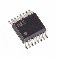
MAX1167BEEE+ Maxim Integrated Products, MAX1167BEEE+ Datasheet - Page 6

MAX1167BEEE+
Manufacturer Part Number
MAX1167BEEE+
Description
IC ADC 16BIT 200KSPS 16-QSOP
Manufacturer
Maxim Integrated Products
Datasheet
1.MAX1167BEEE.pdf
(30 pages)
Specifications of MAX1167BEEE+
Number Of Bits
16
Sampling Rate (per Second)
200k
Data Interface
MICROWIRE™, QSPI™, Serial, SPI™
Number Of Converters
1
Power Dissipation (max)
667mW
Voltage Supply Source
Analog and Digital
Operating Temperature
-40°C ~ 85°C
Mounting Type
Surface Mount
Package / Case
16-SSOP (0.150", 3.90mm Width)
Lead Free Status / RoHS Status
Lead free / RoHS Compliant
Multichannel, 16-Bit, 200ksps Analog-to-Digital
Converters
TIMING CHARACTERISTICS (Figures 1, 2, 8, and 16)
(AV
(200ksps), external V
Note 1:
Note 2:
Note 3:
Note 4:
Note 5:
Note 6:
Note 7:
Note 8:
Note 9:
Note 10: Defined as the change in the positive full scale caused by a ±5% variation in the nominal supply voltage.
6
Acquisition Time
SCLK to DOUT Valid
CS Fall to DOUT Enable
CS Rise to DOUT Disable
CS Pulse Width
CS to SCLK Setup
CS to SCLK Hold
SCLK High Pulse Width
SCLK Low Pulse Width
SCLK Period
DIN to SCLK Setup
DIN to SCLK Hold
CS Falling to DSPR Rising
DSPR to SCLK Falling Setup
DSPR to SCLK Falling Hold
DD
_______________________________________________________________________________________
= +4.75V to +5.25V, DV
AV
Relative accuracy is the deviation of the analog value at any code from its theoretical value after full-scale range has been
calibrated.
Offset and reference errors nulled.
DC voltage applied to on channel, and a full-scale 1kHz sine wave applied to off channels.
Conversion time is measured from the rising edge of the 8th external SCLK pulse to EOC transition minus t
data-transfer mode.
See Figures 10 and 17.
f
n
Guaranteed by design; not production tested.
Internal reference and buffer are left on between conversions.
PARAMETER
SCLK
1
DD
= number of scans, n
= DV
= 4.8MHz, f
REF
DD
= +4.096V, T
= +5.0V.
INTCLK
DD
2
= 4.0MHz. Sample rate is calculated with the formula f
= number of SCLK cycles, and n
= +2.7V to +5.25V, f
SYMBOL
A
t
t
= T
t
t
t
t
ACQ
t
CSW
CSH
t
t
t
t
CSS
t
t
t
t
FSH
FSS
DO
CH
DH
DV
CL
CP
DS
DF
TR
MIN
to T
External clock (Note 6)
C
C
C
SCLK rise
SCLK fall (DSP)
SCLK rise
SCLK fall (DSP)
Duty cycle 45% to 55%
Duty cycle 45% to 55%
SCLK rise
SCLK fall (DSP)
SCLK rise
SCLK fall (DSP)
MAX
DOUT
DOUT
DOUT
, unless otherwise noted. Typical values are at T
= 30pF
= 30pF
= 30pF
SCLK
= 4.8MHz external clock (50% duty cycle), 24 clocks/conversion
CONDITIONS
3
= number of internal clock cycles (see Figures 11–14).
Conversion
Data transfer
Conversion
Data transfer
s
= n
1
(n
MIN
729
100
100
209
100
100
100
2
93
93
93
93
0
0
0
/ f
SCLK
A
= +25°C.)
TYP
+ n
3
/ f
INTCLK
MAX
ACQ
100
100
80
) -1 where:
in 8-bit
UNITS
ns
ns
ns
ns
ns
ns
ns
ns
ns
ns
ns
ns
ns
ns
ns


