LTC2172CUKG-14#PBF Linear Technology, LTC2172CUKG-14#PBF Datasheet - Page 18
LTC2172CUKG-14#PBF
Manufacturer Part Number
LTC2172CUKG-14#PBF
Description
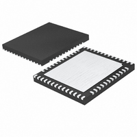
IC ADC 14BIT SER/PAR 65M 52-QFN
Manufacturer
Linear Technology
Datasheet
1.LTC2172IUKG-14PBF.pdf
(34 pages)
Specifications of LTC2172CUKG-14#PBF
Number Of Bits
14
Sampling Rate (per Second)
65M
Data Interface
Serial, Parallel
Number Of Converters
4
Power Dissipation (max)
419mW
Voltage Supply Source
Analog and Digital
Operating Temperature
0°C ~ 70°C
Mounting Type
Surface Mount
Package / Case
52-WFQFN Exposed Pad
Lead Free Status / RoHS Status
Lead free / RoHS Compliant


PIN FUNCTIONS
LTC2172-14/
LTC2171-14/LTC2170-14
mode (PAR/SER = V
internal 100Ω termination resistors on the digital out-
puts. When used as an input, SDO can be driven with
1.8V to 3.3V logic through a 1k series resistor.
PAR/SER (Pin 47): Programming Mode Selection Pin.
Connect to ground to enable serial programming mode.
CS, SCK, SDI and SDO become a serial interface that con-
trols the A/D operating modes. Connect to V
parallel programming mode where CS, SCK, SDI and SDO
become parallel logic inputs that control a reduced set of
the A/D operating modes. PAR/SER should be connected
directly to ground or the V
by a logic signal.
V
with a 1μF ceramic capacitor, nominally 1.25V.
SENSE (Pin 50): Reference Programming Pin. Connect-
ing SENSE to V
±1V input range. Connecting SENSE to ground selects
the internal reference and a ±0.5V input range. An external
reference between 0.625V and 1.3V applied to SENSE
selects an input range of ±0.8 • V
18
REF
(Pin 48): Reference Voltage Output. Bypass to ground
DD
selects the internal reference and a
DD
), SDO is an input that enables
DD
of the part and not be driven
SENSE
.
DD
to enable
LVDS OUTPUTS
The following pins are differential LVDS outputs. The
output current level is programmable. There is an op-
tional internal 100Ω termination resistor between the
pins of each LVDS output pair.
OUT4B
Pins 25/ 26): Serial Data Outputs for Channel 4. In 1-lane
output mode, only OUT4A
OUT3B
Pins 29/30): Serial Data Outputs for Channel 3. In
1-lane output mode, only OUT3A
FR
DCO
OUT2B
Pins 39/40): Serial Data Outputs for Channel 2. In
1-lane output mode, only OUT2A
OUT2B
Pins 43/44): Serial Data Outputs for Channel 1. In
1-lane output mode, only OUT1A
–
/FR
–
/DCO
+
–
–
–
–
/OUT4B
/OUT3B
(Pin 31/Pin 32): Frame Start Output.
/OUT2B
/OUT2B
+
(Pin 35/Pin 36): Data Clock Output.
+
+
+
+
, OUT4A
, OUT3A
, OUT2A
, OUT2A
–
/OUT4A
–
–
–
–
/OUT4A
/OUT3A
/OUT2A
/OUT2A
–
–
–
/OUT3A
/OUT2A
/OUT1A
+
are used.
+
+
+
+
(Pins 23/24,
(Pins 27/28,
(Pins 37/38,
(Pins 41/42,
+
+
+
are used.
are used.
are used.
21721014fa
Related parts for LTC2172CUKG-14#PBF
Image
Part Number
Description
Manufacturer
Datasheet
Request
R

Part Number:
Description:
IC ADC 12BIT SER/PAR 65M 52-QFN
Manufacturer:
Linear Technology
Datasheet:
Part Number:
Description:
IC ADC 12BIT SER/PAR 65M 52-QFN
Manufacturer:
Linear Technology
Datasheet:
Part Number:
Description:
IC ADC 14BIT SER/PAR 65M 52-QFN
Manufacturer:
Linear Technology
Datasheet:

Part Number:
Description:
14-Bit, 65Msps/40Msps/25Msps Low Power Quad ADCs
Manufacturer:
LINER [Linear Technology]
Datasheet:

Part Number:
Description:
CD ROM LINEARVIEW DATASHEETS
Manufacturer:
Linear Technology

Part Number:
Description:
Standalone Linear Li-Ion Battery Charger with Thermal Regulation in ThinSOT
Manufacturer:
Linear Technology Corporation
Datasheet:
Part Number:
Description:
Low noise, high frequency, 8th order linear phase lowpass filter
Manufacturer:
Linear Technology Corporation
Datasheet:
Part Number:
Description:
Manufacturer:
Linear Technology Corporation
Datasheet:
Part Number:
Description:
Manufacturer:
Linear Technology Corporation
Datasheet:
Part Number:
Description:
Manufacturer:
Linear Technology Corporation
Datasheet:
Part Number:
Description:
Manufacturer:
Linear Technology Corporation
Datasheet:
Part Number:
Description:
Manufacturer:
Linear Technology Corporation
Datasheet:
Part Number:
Description:
Manufacturer:
Linear Technology Corporation
Datasheet:
Part Number:
Description:
Manufacturer:
Linear Technology Corporation
Datasheet:
Part Number:
Description:
Dual and Quad, JFET Input Precision High Speed Op Amps
Manufacturer:
Linear Technology Corporation
Datasheet: