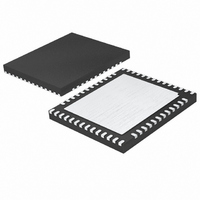
LTC2172CUKG-14#PBF Linear Technology, LTC2172CUKG-14#PBF Datasheet - Page 26

LTC2172CUKG-14#PBF
Manufacturer Part Number
LTC2172CUKG-14#PBF
Description
IC ADC 14BIT SER/PAR 65M 52-QFN
Manufacturer
Linear Technology
Datasheet
1.LTC2172IUKG-14PBF.pdf
(34 pages)
Specifications of LTC2172CUKG-14#PBF
Number Of Bits
14
Sampling Rate (per Second)
65M
Data Interface
Serial, Parallel
Number Of Converters
4
Power Dissipation (max)
419mW
Voltage Supply Source
Analog and Digital
Operating Temperature
0°C ~ 70°C
Mounting Type
Surface Mount
Package / Case
52-WFQFN Exposed Pad
Lead Free Status / RoHS Status
Lead free / RoHS Compliant
LTC2172-14/
LTC2171-14/LTC2170-14
APPLICATIONS INFORMATION
The fi rst bit of the 16-bit input word is the R/W bit. The
next seven bits are the address of the register (A6:A0).
The fi nal eight bits are the register data (D7:D0).
If the R/W bit is low, the serial data (D7:D0) will be written
to the register set by the address bits (A6:A0). If the R/W
bit is high, data in the register set by the address bits (A6:
A0) will be read back on the SDO pin (see the Timing Dia-
grams section). During a readback command the register
is not updated and data on SDI is ignored.
The SDO pin is an open-drain output that pulls to ground
with a 200Ω impedance. If register data is read back through
SDO, an external 2k pull-up resistor is required. If serial
Table 4. Serial Programming Mode Register Map (PAR/SER = GND)
REGISTER A0: RESET REGISTER (ADDRESS 00h)
REGISTER A1: POWER-DOWN REGISTER (ADDRESS 01h)
26
Bit 7
Bits 6-0
Bit 7
Bit 6
Bit 5
Bits 4-0
DCSOFF
RESET
D7
D7
RESET
0 = Not Used
1 = Software Reset. All Mode Control Registers Are Reset to 00h. The ADC is momentarily placed in SLEEP mode. This Bit Is
Automatically Set Back to Zero After the Reset Is Complete
Unused, Don’t Care Bits.
DCSOFF
0 = Clock Duty Cycle Stabilizer On
1 = Clock Duty Cycle Stabilizer Off. This is Not Recommended.
RAND
0 = Data Output Randomizer Mode Off
1 = Data Output Randomizer Mode On
TWOSCOMP
0 = Offset Binary Data Format
1 = Two’s Complement Data Format
SLEEP:NAP_4:NAP_1
00000 = Normal Operation
0XXX1 = Channel 1 in Nap Mode
0XX1X = Channel 2 in Nap Mode
0X1XX = Channel 3 in Nap Mode
01XXX = Channel 4 in Nap Mode
1XXXX = Sleep Mode. All Channels Are Disabled
Note: Any Combination of Channels Can Be Placed in Nap Mode.
RAND
D6
D6
X
Clock Duty Cycle Stabilizer Bit
Data Output Randomizer Mode Control Bit
Software Reset Bit
Two’s Complement Mode Control Bit
TWOSCOMP
D5
D5
X
Sleep/Nap Mode Control Bits
SLEEP
D4
D4
X
data is only written and readback is not needed, then SDO
can be left fl oating and no pull-up resistor is needed. Table
4 shows a map of the mode control registers.
Software Reset
If serial programming is used, the mode control registers
should be programmed as soon as possible after the power
supplies turn on and are stable. The fi rst serial command
must be a software reset which will reset all register data
bits to logic 0. To perform a software reset, bit D7 in the
reset register is written with a logic 1. After the reset is
complete, bit D7 is automatically set back to zero.
NAP_4
D3
D3
X
NAP_3
D2
D2
X
NAP_2
D1
D1
X
NAP_1
D0
D0
X
21721014fa


