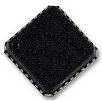
AD7194BCPZ Analog Devices Inc, AD7194BCPZ Datasheet - Page 11

AD7194BCPZ
Manufacturer Part Number
AD7194BCPZ
Description
IC ADC 24BIT SPI 4.8K 32-LFCSP
Manufacturer
Analog Devices Inc
Datasheet
1.AD7194BCPZ.pdf
(56 pages)
Specifications of AD7194BCPZ
Data Interface
DSP, MICROWIRE™, QSPI™, Serial, SPI™
Number Of Bits
24
Sampling Rate (per Second)
4.8k
Number Of Converters
1
Voltage Supply Source
Analog and Digital
Operating Temperature
-40°C ~ 105°C
Mounting Type
Surface Mount
Package / Case
32-WFQFN, CSP Exposed Pad
Resolution (bits)
24bit
Input Channel Type
Pseudo Differential
Supply Voltage Range - Analogue
3V To 5.25V
Supply Voltage Range - Digital
2.7V To 5.25V
Supply
RoHS Compliant
Sampling Rate
4.8kSPS
Rohs Compliant
Yes
Lead Free Status / RoHS Status
Lead free / RoHS Compliant
Other names
AD7194BRUZ
AD7194BRUZ
AD7194BRUZ
Available stocks
Company
Part Number
Manufacturer
Quantity
Price
Part Number:
AD7194BCPZ
Manufacturer:
ADI/亚德诺
Quantity:
20 000
Pin No.
23
24
25
26
27
28
29
30
31
32
Mnemonic
AV
DV
SYNC
NC
DOUT/RDY
DIN
MCLK1
MCLK2
SCLK
CS
DD
DD
This pin should be connected to GND for correct operation.
Description
Analog Supply Voltage, 3 V to 5.25 V. AV
with AV
Digital Supply Voltage, 2.7 V to 5.25 V. DV
with DV
Logic input that allows for synchronization of the digital filters and analog modulators when using a
number of AD7194 devices. While SYNC is low, the nodes of the digital filter, the filter control logic, and the
calibration control logic are reset, and the analog modulator is also held in its reset state. SYNC does not
affect the digital interface but does reset RDY to a high state if it is low. SYNC has a pull-up resistor
internally to DV
Serial Data Output/Data Ready Output. DOUT/RDY serves a dual purpose. It functions as a serial data
output pin to access the output shift register of the ADC. The output shift register can contain data from
any of the on-chip data or control registers. In addition, DOUT/RDY operates as a data ready pin, going low
to indicate the completion of a conversion. If the data is not read after the conversion, the pin goes high
before the next update occurs. The DOUT/RDY falling edge can be used as an interrupt to a processor,
indicating that valid data is available. With an external serial clock, the data can be read using the
DOUT/RDY pin. With CS low, the data-/control-word information is placed on the DOUT/RDY pin on the
SCLK falling edge and is valid on the SCLK rising edge.
Serial Data Input to the Input Shift Register on the ADC. Data in this shift register is transferred to the
control registers in the ADC, with the register selection bits of the communications register identifying the
appropriate register.
When the master clock for the device is provided externally by a crystal, the crystal is connected between
MCLK1 and MCLK2.
Master Clock Signal for the Device. The AD7194 has an internal 4.92 MHz clock. This internal clock can be
made available on the MCLK2 pin. The clock for the AD7194 can also be provided externally in the form of
a crystal or external clock. A crystal can be tied across the MCLK1 and MCLK2 pins. Alternatively, the MCLK2
pin can be driven with a CMOS-compatible clock and with the MCLK1 pin remaining unconnected.
Serial Clock Input. This serial clock input is for data transfers to and from the ADC. The SCLK has a Schmitt-
triggered input, making the interface suitable for opto-isolated applications. The serial clock can be
continuous with all data transmitted in a continuous train of pulses. Alternatively, it can be a nonconti-
nuous clock with the information transmitted to or from the ADC in smaller batches of data.
Chip Select Input. This is an active low logic input used to select the ADC. CS can be used to select the
ADC in systems with more than one device on the serial bus or as a frame synchronization signal in
communicating with the device. CS can be hardwired low, allowing the ADC to operate in 3-wire mode
with SCLK, DIN, and DOUT used to interface with the device.
DD
DD
at 5 V or vice versa.
at 5 V or vice versa.
DD
.
Rev. 0 | Page 11 of 56
DD
DD
is independent of DV
is independent of AV
DD
DD
. Therefore, DV
. Therefore, AV
DD
DD
can be operated at 3 V
can be operated at 3 V
AD7194


