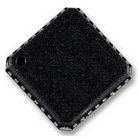
AD7194BCPZ Analog Devices Inc, AD7194BCPZ Datasheet - Page 30

AD7194BCPZ
Manufacturer Part Number
AD7194BCPZ
Description
IC ADC 24BIT SPI 4.8K 32-LFCSP
Manufacturer
Analog Devices Inc
Datasheet
1.AD7194BCPZ.pdf
(56 pages)
Specifications of AD7194BCPZ
Data Interface
DSP, MICROWIRE™, QSPI™, Serial, SPI™
Number Of Bits
24
Sampling Rate (per Second)
4.8k
Number Of Converters
1
Voltage Supply Source
Analog and Digital
Operating Temperature
-40°C ~ 105°C
Mounting Type
Surface Mount
Package / Case
32-WFQFN, CSP Exposed Pad
Resolution (bits)
24bit
Input Channel Type
Pseudo Differential
Supply Voltage Range - Analogue
3V To 5.25V
Supply Voltage Range - Digital
2.7V To 5.25V
Supply
RoHS Compliant
Sampling Rate
4.8kSPS
Rohs Compliant
Yes
Lead Free Status / RoHS Status
Lead free / RoHS Compliant
Other names
AD7194BRUZ
AD7194BRUZ
AD7194BRUZ
Available stocks
Company
Part Number
Manufacturer
Quantity
Price
Part Number:
AD7194BCPZ
Manufacturer:
ADI/亚德诺
Quantity:
20 000
AD7194
ANALOG INPUT CHANNEL
The AD7194 uses flexible multiplexing so any of the analog
input pins AIN1 to AIN16 can be selected as a positive input or
a negative input (see Table 22 and Table 23). The AINCOM pin
can be a negative analog input pin only.
The channels are configured using bits CH7 to CH0 and bit
Pseudo in the configuration register (See Table 22 to Table 24).
The device can be configured to have eight differential inputs,
sixteen pseudo-differential inputs or a combination of both. The
inputs can be buffered or unbuffered. In the buffered mode (the
BUF bit in the configuration register is set to 1), the input channel
feeds into a high impedance input stage of the buffer amplifier.
Therefore, the input can tolerate significant source impedances and
is tailored for direct connection to external resistive type sensors
such as strain gages or resistance temperature detectors (RTDs).
When BUF = 0, the part is operated in the unbuffered mode.
This results in a higher analog input current. Note that this
unbuffered input path provides a dynamic load to the driving
source. Therefore, resistor/capacitor combinations on the input
pins can cause gain errors, depending on the output impedance
of the source that is driving the ADC input. Table 26 shows the
allowable external resistance/capacitance values for unbuffered
mode at a gain of 1 such that no gain error at the 18-bit level is
introduced.
Table 26. External R-C Combination for No 18-Bit Gain Error
C (pF)
50
100
500
1000
5000
AINCOM
AIN15
AIN16
AIN1
AIN2
Figure 22. Analog Input Multiplexer Circuit
AVDD
AVDD
AVDD
AVDD
AVDD
R (Ω)
1.4 k
850
300
230
30
AVDD
CURRENTS
BURNOUT
PGA
TO ADC
Rev. 0 | Page 30 of 56
The absolute input voltage range in buffered mode is restricted
to a range between AGND + 250 mV and AV
must be taken in setting up the common-mode voltage to not
exceed these limits; otherwise, linearity and noise performance
degrade.
The absolute input voltage in unbuffered mode includes the
range between AGND − 50 mV and AV
negative absolute input voltage limit allows the possibility of
monitoring small true bipolar signals with respect to AGND.
PROGRAMMABLE GAIN ARRAY (PGA)
When the gain stage is enabled, the output from the buffer is
applied to the input of the PGA. The presence of the PGA
means that signals of small amplitude can be gained within the
AD7194 and still maintain excellent noise performance. For
example, when the gain is set to 128, the rms noise is 11 nV,
typically, when the output data rate is 4.7 Hz, which is equivalent
to 22.7 bits of effective resolution or 20 bits of noise-free
resolution.
The AD7194 can be programmed to have a gain of 1, 8, 16,
32, 64, and 128 by using Bit G2 to Bit G0 in the configuration
register. Therefore, with an external 2.5 V reference, the
unipolar ranges are from 0 mV to 19.53 mV to 0 V to 2.5 V,
and the bipolar ranges are from ±19.53 mV to ±2.5 V.
The analog input range must be limited to ±(AV
because the PGA requires some headroom. Therefore, if V
AV
AD7194 is 0 V to 3.75 V/gain in unipolar mode or ±3.75 V/gain
in bipolar mode.
REFERENCE
The ADC has a fully differential input capability for the
reference channel. In addition, the user has the option of
selecting one of two external reference options (REFIN1(±)
or REFIN2(±)). The reference source for the AD7194 is
selected using the REFSEL bit in the configuration register.
The REFIN2(±) pins are dual purpose: they can function as
two general-purpose output pins or as reference pins. When
the REFSEL bit is set to 1, these pins automatically function as
reference pins.
The common-mode range for these differential inputs is from
AGND to AV
REFINx(−)) is AV
with reference voltages from 1 V to AV
the excitation (voltage or current) for the transducer on the
analog input also drives the reference voltage for the part, the
effect of the low frequency noise in the excitation source is removed
because the application is ratiometric. If the AD7194 is used in a
nonratiometric application, a low noise reference should be used.
The reference input is unbuffered; therefore, excessive R-C
source impedances introduce gain errors. R-C values similar to
those in Table 26 are recommended for the reference inputs.
Deriving the reference input voltage across an external resistor
means that the reference input sees significant external source
DD
= 5 V, the maximum analog input that can be applied to the
DD
. The reference voltage REFIN (REFINx(+) −
DD
nominal, but the AD7194 is functional
DD
DD
. In applications where
+ 50 mV. The
DD
DD
− 250 mV. Care
− 1.25 V)/gain
REF
=


