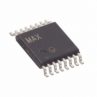
MAX1415EUE+ Maxim Integrated Products, MAX1415EUE+ Datasheet - Page 19

MAX1415EUE+
Manufacturer Part Number
MAX1415EUE+
Description
IC ADC 16BIT DELTA SIGMA 16TSSOP
Manufacturer
Maxim Integrated Products
Datasheet
1.MAX1415EUE.pdf
(36 pages)
Specifications of MAX1415EUE+
Number Of Bits
16
Sampling Rate (per Second)
500
Data Interface
MICROWIRE™, QSPI™, Serial, SPI™
Number Of Converters
1
Power Dissipation (max)
755mW
Voltage Supply Source
Single Supply
Operating Temperature
-45°C ~ 85°C
Mounting Type
Surface Mount
Package / Case
16-TSSOP
Lead Free Status / RoHS Status
Lead free / RoHS Compliant
The MAX1415/MAX1416 low-power, 2-channel serial
output ADCs use a sigma-delta modulator with a digital
filter to achieve 16-bit resolution with no missing codes.
Each device includes a PGA, an on-chip input buffer,
an internal oscillator, and a bidirectional communica-
tions port. The MAX1415 operates with a 2.7V to 3.6V
single supply, and the MAX1416 operates with a 4.75V
to 5.25V single supply.
Fully differential inputs, an internal input buffer, and an
on-chip PGA (gain = 1 to 128) allow low-level signals to
be directly measured, minimizing the requirements for
external signal conditioning. Self-calibration corrects for
gain and offset errors. A programmable digital filter
allows for the selection of the output data rate and first
notch frequency from 20Hz to 500Hz.
The bidirectional serial SPI-/QSPI-/MICROWIRE-compati-
ble interface consists of four digital control lines (SCLK,
CS, DOUT, and DIN) and provides an easy interface to
microcontrollers (µCs). Connect CS to GND to configure
the MAX1415/MAX1416 for 3-wire operation.
AIN1+
AIN2+
AIN1-
AIN2-
REF+
REF-
______________________________________________________________________________________
Detailed Description
MUX
BUFFERED MODE AND CLOSED
S1 AND S2 ARE OPEN IN
IN UNBUFFERED MODE
BUFFER
BUFFER
16-Bit, Low-Power, 2-Channel,
S2
S1
MAX1415
MAX1416
PGA
The MAX1415/MAX1416 accept four analog inputs
(AIN1+, AIN1-, AIN2+, and AIN2-) in buffered or
unbuffered mode. Use
and negative input pair for a fully differential channel.
The input buffer isolates the inputs from the capacitive
load presented by the PGA/modulator, allowing for high
source-impedance analog transducers. The value of
the BUF bit in the setup register (see the Setup Register
section) determines whether the input buffer is enabled
or disabled.
Internal protection diodes, which clamp the analog
input to V
(GND - 0.3V) to (V
device. If the analog input exceeds 300mV beyond the
supplies, limit the input current to 10mA.
When the analog input buffer is disabled, the analog
input drives a typical 7pF (gain = 1) capacitor, C
in series with the 7kΩ typical on-resistance of the track
and hold (T/H) switch (Figure 1). C
of the sampling capacitor, C
itance, C
to (AIN+ - AIN-). The gain determines the value of
C
SAMP
SIGMA-DELTA
MODULATOR
2nd-ORDER
(see Table 5).
STRAY
DD
GENERATOR
Sigma-Delta ADCs
CLOCK
SERIAL INTERFACE,
and/or GND, allow the input to swing from
REGISTERS,
. During the conversion, C
CONTROL
AND
DIGITAL
FILTER
DD
+ 0.3V), without damaging the
Functional Diagram
Table 8 to select the positive
SAMP
, and the stray capac-
CLKIN
CLKOUT
V
GND
CS
SCLK
DIN
DOUT
DRDY
RESET
TOTAL
DD
Analog Inputs
Input Buffers
SAMP
is comprised
charges
TOTAL
19
,


