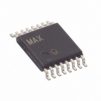
MAX1415EUE+ Maxim Integrated Products, MAX1415EUE+ Datasheet - Page 26

MAX1415EUE+
Manufacturer Part Number
MAX1415EUE+
Description
IC ADC 16BIT DELTA SIGMA 16TSSOP
Manufacturer
Maxim Integrated Products
Datasheet
1.MAX1415EUE.pdf
(36 pages)
Specifications of MAX1415EUE+
Number Of Bits
16
Sampling Rate (per Second)
500
Data Interface
MICROWIRE™, QSPI™, Serial, SPI™
Number Of Converters
1
Power Dissipation (max)
755mW
Voltage Supply Source
Single Supply
Operating Temperature
-45°C ~ 85°C
Mounting Type
Surface Mount
Package / Case
16-TSSOP
Lead Free Status / RoHS Status
Lead free / RoHS Compliant
The byte-wide clock register is bidirectional, so it can
be written and read. The byte written to the setup regis-
ter sets the clock, filter first notch frequency, and the
output data rate (see
MXID: (Default = 1) Maxim-Identifier Bit. This is a read-
only bit. Values written to this bit are ignored.
ZERO: (Default = 0) Zero Bit. This is a read-only bit.
Values written to this bit are ignored.
16-Bit, Low-Power, 2-Channel,
Sigma-Delta ADCs
Table 10. Operating-Mode Selection
Table 11. PGA Gain Selection
26
MD1
0
0
1
1
______________________________________________________________________________________
G2
0
0
0
0
1
1
1
1
MD0
0
1
0
1
G1
0
0
1
1
0
0
1
1
Normal Mode. Use this mode to perform normal conversions on the selected analog input channel.
Self-Calibration Mode. This mode performs self-calibration on the selected channel determined from CH0 and
CH1 selection bits in the communications register (Table 6). Upon completion of self-calibration, the device
returns to normal mode with MD1, MD0 returning to 0, 0. The DRDY output bit goes high when self-calibration is
requested and returns low when the calibration is complete and a new data word is in the data register. Self-
calibration performs an internal zero-scale and full-scale calibration. The analog inputs of the device are shorted
together internally during zero-scale calibration and connected to an internally generated (V
during full-scale calibration. The offset and gain registers for the selected channel are automatically updated
with the calibration data.
Zero-Scale System-Calibration Mode. This mode performs zero-scale calibration on the selected channel
determined from CH1 and CH0 selection bits in the communications register (Table 6). The DRDY output bit
goes high when calibration is requested and returns low when the calibration is complete and a new data word
is in the data register. Performing zero-scale calibration compensates for any DC offset voltage present in the
ADC and system. Ensure that the analog input voltage is stable within 0.5 LSB for the duration of the calibration
sequence. The offset register for the selected channel is updated with the zero-scale system-calibration data.
Upon completion of calibration, the device returns to normal mode with MD1, MD0 returning to 0, 0.
Full-Scale System-Calibration Mode. This mode performs full-scale system-calibration on the selected channel
determined from CH1 and CH0 selection bits in the communications register. This calibration assigns a full-
scale output code to the voltage present on the selected channel. Ensure that the analog input voltage is stable
within 0.5 LSB for the duration of the calibration sequence. The DRDY output bit goes high during calibration
and returns low when the calibration is complete and a new data word is in the data register. The gain register
for the selected channel is updated with the full-scale system-calibration data. Upon completion of calibration,
the device returns to normal mode with MD1, MD0 returning to 0, 0.
Table 12).
G0
0
1
0
1
0
1
0
1
Clock Register
PGA GAIN
128
16
32
64
1
2
4
8
OPERATING MODE
INTCLK: (Default = 0) Internal Oscillator Bit. Set INTCLK
= 1 to enable the internal oscillator. Set INTCLK = 0 to
disable the internal oscillator.
CLKDIS: (Default = 0) Clock-Disable Bit. Set CLKDIS = 1
to disable the internally or externally generated clock from
appearing on CLKOUT. When using a crystal or res-
onator across CLKIN and CLKOUT, the clock is stopped
and no conversions take place when CLKDIS = 1.
CLKOUT is held low during clock disable to save power.
Set CLKDIS = 0 to allow other devices to use the output
signal on CLKOUT as a clock source and/or to enable the
external oscillator. The CLKOUT pin on the MAX1415/
MAX1416 can drive one CMOS load.
CLKDIV: (Default = 0) Clock-Divider Control Bit. The
MAX1415/MAX1416 each have an internal clock divider.
Set this bit to 1 to divide the input clock by two. When this
bit is set to 0, the MAX1415/MAX1416 operate at the
internal or external oscillator frequency. CLKDIV has no
effect on the internal oscillator.
CLK: (Default = 1) Clock Bit. When using the internal
oscillator (INTCLK = 1), set CLK = 1 for a frequency of
2.4576MHz, and set CLK = 0 for a frequency of 1MHz.
When using an external clock/oscillator, set CLK = 1 for
f
4.9152MHz with CLKDIV = 1.
CLKIN
= 2.4576MHz with CLKDIV = 0, or f
REF
/GAIN) voltage
CLKIN
=


