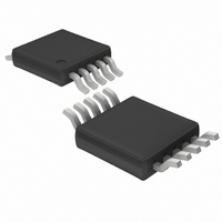
LTC2402CMS Linear Technology, LTC2402CMS Datasheet - Page 11

LTC2402CMS
Manufacturer Part Number
LTC2402CMS
Description
IC ADC 24BIT 2CH MICROPWR 10MSOP
Manufacturer
Linear Technology
Datasheet
1.LTC2401CMSPBF.pdf
(32 pages)
Specifications of LTC2402CMS
Number Of Bits
24
Sampling Rate (per Second)
7.5
Data Interface
MICROWIRE™, Serial, SPI™
Number Of Converters
2
Power Dissipation (max)
1mW
Voltage Supply Source
Single Supply
Operating Temperature
0°C ~ 70°C
Mounting Type
Surface Mount
Package / Case
10-TFSOP, 10-MSOP (0.118", 3.00mm Width)
Lead Free Status / RoHS Status
Contains lead / RoHS non-compliant
Available stocks
Company
Part Number
Manufacturer
Quantity
Price
Company:
Part Number:
LTC2402CMS
Manufacturer:
LT
Quantity:
10 000
Part Number:
LTC2402CMS
Manufacturer:
LINEAR/凌特
Quantity:
20 000
Part Number:
LTC2402CMS#PBF
Manufacturer:
LINEAR/凌特
Quantity:
20 000
APPLICATIO S I FOR ATIO
integrity of the conversion result and of the serial interface
mode selection which is performed at the initial power-up.
(See the 2-wire I/O sections in the Serial Interface Timing
Modes section.)
When the V
the converter creates an internal power-on-reset (POR)
signal with duration of approximately 0.5ms. The POR
signal clears all internal registers. Following the POR
signal, the LTC2401/LTC2402 start a normal conversion
cycle and follows the normal succession of states de-
scribed above. The first conversion result following POR
is accurate within the specifications of the device.
Reference Voltage Range
The LTC2401/LTC2402 can accept a reference voltage
(V
output noise is determined by the thermal noise of the
front-end circuits, and as such, its value in microvolts is
nearly constant with reference voltage. A decrease in
reference voltage will not significantly improve the
converter’s effective resolution. On the other hand, a
reduced reference voltage will improve the overall con-
verter INL performance. The recommended range for the
LTC2401/LTC2402 voltage reference is 100mV to V
Input Voltage Range
The converter is able to accommodate system level
offset and gain errors as well as system level overrange
situations due to its extended input range, see Figure 2.
The LTC2401/LTC2402 convert input signals within the
extended input range of – 0.125 • V
(V
For large values of V
is limited by the absolute maximum voltage range of
– 0.3V to (V
protection devices begin to turn on and the errors due to
the input leakage current increase rapidly.
Input signals applied to V
– 300mV and above V
fault current, a resistor of up to 5k may be added in series
with the V
device. In the physical layout, it is important to maintain
REF
REF
= FS
= FS
IN
SET
SET
CC
CC
pin without affecting the performance of the
voltage rises above this critical threshold,
+ 0.3V). Beyond this range, the input ESD
– ZS
– ZS
U
SET
REF
SET
CC
).
(V
) from 0V to V
by 300mV. In order to limit any
IN
REF
U
may extend below ground by
= FS
SET
W
REF
– ZS
CC
to 1.125 • V
. The converter
SET
), this range
U
CC
REF
.
the parasitic capacitance of the connection between this
series resistance and the V
therefore, the resistor should be located as close as
practical to the V
on the converter accuracy can be evaluated from the
curves presented in the Analog Input/Reference Current
section. In addition, a series resistor will introduce a
temperature dependent offset error due to the input leak-
age current. A 1nA input leakage current will develop a
1ppm offset error on a 5k resistor if V
has a very strong temperature dependency.
Output Data Format
The LTC2401/LTC2402 serial output data stream is 32 bits
long. The first 4 bits represent status information indicat-
ing the sign, selected channel, input range and conversion
state. The next 24 bits are the conversion result, MSB first.
The remaining 4 bits are sub LSBs beyond the 24-bit level
that may be included in averaging or discarded without
loss of resolution.
Bit 31 (first output bit) is the end of conversion (EOC)
indicator. This bit is available at the SDO pin during the
conversion and sleep states whenever the CS pin is LOW.
This bit is HIGH during the conversion and goes LOW when
the conversion is complete.
Bit 30 (second output bit) for the LTC2402, this bit is LOW
if the last conversion was performed on CH0 and HIGH for
CH1. This bit is always low for the LTC2401.
FS
ZS
SET
SET
V
+ 0.12V
– 0.12V
CC
+ 0.3V
ZS
FS
–0.3V
Figure 2. LTC2401/LTC2402 Input Range
REF
SET
SET
REF
(V
REF
IN
= FS
NORMAL
pin. The effect of the series resistance
RANGE
INPUT
SET
LTC2401/LTC2402
– ZS
SET
EXTENDED
RANGE
INPUT
IN
)
pin as low as possible;
ABSOLUTE
MAXIMUM
REF
RANGE
INPUT
24012 F02
= 5V. This error
11


