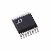
LTC2415-1CGN Linear Technology, LTC2415-1CGN Datasheet - Page 18

LTC2415-1CGN
Manufacturer Part Number
LTC2415-1CGN
Description
IC ADC 24BIT DIFFINPUT/REF16SSOP
Manufacturer
Linear Technology
Datasheet
1.LTC2415CGNPBF.pdf
(40 pages)
Specifications of LTC2415-1CGN
Number Of Bits
24
Sampling Rate (per Second)
13.75
Data Interface
MICROWIRE™, Serial, SPI™
Number Of Converters
2
Power Dissipation (max)
1mW
Voltage Supply Source
Single Supply
Operating Temperature
0°C ~ 70°C
Mounting Type
Surface Mount
Package / Case
16-SSOP (0.150", 3.90mm Width)
Lead Free Status / RoHS Status
Contains lead / RoHS non-compliant
Available stocks
Company
Part Number
Manufacturer
Quantity
Price
Company:
Part Number:
LTC2415-1CGN
Manufacturer:
LT
Quantity:
10 000
Part Number:
LTC2415-1CGN
Manufacturer:
LINEAR/凌特
Quantity:
20 000
Company:
Part Number:
LTC2415-1CGN#PBF
Manufacturer:
TI
Quantity:
120
Part Number:
LTC2415-1CGN#PBF
Manufacturer:
LINEAR/凌特
Quantity:
20 000
Part Number:
LTC2415-1CGN#TRPBF
Manufacturer:
LINEAR/凌特
Quantity:
20 000
LTC2415/LTC2415-1
APPLICATIO S I FOR ATIO
Serial Clock Input/Output (SCK)
The serial clock signal present on SCK (Pin 13) is used to
synchronize the data transfer. Each bit of data is shifted out
the SDO pin on the falling edge of the serial clock.
In the Internal SCK mode of operation, the SCK pin is an
output and the LTC2415/LTC2415-1 create their own se-
rial clock by dividing the internal conversion clock by 8. In
the External SCK mode of operation, the SCK pin is used
as input. The internal or external SCK mode is selected on
power-up and then reselected every time a HIGH-to-LOW
transition is detected at the CS pin. If SCK is HIGH or float-
ing at power-up or during this transition, the converter
enters the internal SCK mode. If SCK is LOW at power-up
or during this transition, the converter enters the external
SCK mode.
Serial Data Output (SDO)
The serial data output pin, SDO (Pin 12), provides the
result of the last conversion as a serial bit stream (MSB
first) during the data output state. In addition, the SDO pin
is used as an end of conversion indicator during the
conversion and sleep states.
When CS (Pin 11) is HIGH, the SDO driver is switched to
a high impedance state. This allows sharing the serial
interface with other devices. If CS is LOW during the
convert or sleep state, SDO will output EOC. If CS is LOW
during the conversion phase, the EOC bit appears HIGH on
the SDO pin. Once the conversion is complete, EOC goes
LOW. The device remains in the sleep state until the first
rising edge of SCK occurs while CS = LOW.
Chip Select Input (CS)
The active LOW chip select, CS (Pin 11), is used to test the
Table 4. LTC2415/LTC2415-1 Interface Timing Modes
Configuration
External SCK, Single Cycle Conversion
External SCK, 2-Wire I/O
Internal SCK, Single Cycle Conversion
Internal SCK, 2-Wire I/O, Continuous Conversion
Internal SCK, Autostart Conversion
18
U
U
W
External
External
Internal
Internal
Internal
Source
U
SCK
conversion status and to enable the data output transfer as
described in the previous sections.
In addition, the CS signal can be used to trigger a new
conversion cycle before the entire serial data transfer has
been completed. The LTC2415/LTC2415-1 will abort any
serial data transfer in progress and start a new conversion
cycle anytime a LOW-to-HIGH transition is detected at the
CS pin after the converter has entered the data output state
(i.e., after the first rising edge of SCK occurs with
CS = LOW).
Finally, CS can be used to control the free-running modes
of operation, see Serial Interface Timing Modes section.
Grounding CS will force the ADC to continuously convert
at the maximum output rate selected by F
capacitor to CS will reduce the output rate and power
dissipation by a factor proportional to the capacitor’s
value, see Figures 15 to 17.
SERIAL INTERFACE TIMING MODES
The LTC2415/LTC2415-1 3-wire interface is SPI and
MICROWIRE compatible. This interface offers several
flexible modes of operation. These include internal/exter-
nal serial clock, 2- or 3-wire I/O, single cycle conversion
and autostart. The following sections describe each of
these serial interface timing modes in detail. In all these
cases, the converter can use the internal oscillator (F
LOW or F
the F
External Serial Clock, Single Cycle Operation
(SPI/MICROWIRE Compatible)
This timing mode uses an external serial clock to shift out
the conversion result and a CS signal to monitor and
control the state of the conversion cycle, see Figure 8.
Conversion
CS and SCK
Continuous
O
Control
Cycle
CS
SCK
C
pin. Refer to Table 4 for a summary.
EXT
O
= HIGH) or an external oscillator connected to
CS and SCK
Control
Internal
Internal
Output
CS
Data
SCK
Figures 11, 12
Connection
Waveforms
Figures 8, 9
Figure 10
Figure 13
Figure 14
and
O
. Tying a
sn2415 24151fs
O
=


