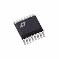
LTC2440IGN#PBF Linear Technology, LTC2440IGN#PBF Datasheet - Page 10

LTC2440IGN#PBF
Manufacturer Part Number
LTC2440IGN#PBF
Description
IC ADC DIFFER 24-BIT HS 16-SSOP
Manufacturer
Linear Technology
Datasheet
1.LTC2440CGN.pdf
(28 pages)
Specifications of LTC2440IGN#PBF
Number Of Bits
24
Sampling Rate (per Second)
3.5k
Data Interface
MICROWIRE™, Serial, SPI™
Number Of Converters
2
Power Dissipation (max)
40mW
Voltage Supply Source
Single Supply
Operating Temperature
-40°C ~ 85°C
Mounting Type
Surface Mount
Package / Case
16-SSOP (0.150", 3.90mm Width)
Lead Free Status / RoHS Status
Lead free / RoHS Compliant
Available stocks
Company
Part Number
Manufacturer
Quantity
Price
LTC2440
APPLICATIONS INFORMATION
Initially, the LTC2440 performs a conversion. Once the
conversion is complete, the device enters the sleep state.
While in this sleep state, power consumption is reduced
below 10μA. The part remains in the sleep state as long
as CS is HIGH. The conversion result is held indefi nitely
in a static shift register while the converter is in the sleep
state.
Once CS is pulled LOW, the device begins outputting the
conversion result. There is no latency in the conversion
result. The data output corresponds to the conversion
just performed. This result is shifted out on the serial data
out pin (SDO) under the control of the serial clock (SCK).
Data is updated on the falling edge of SCK allowing the
user to reliably latch data on the rising edge of SCK (see
Figure 3). The data output state is concluded once 32-bits
are read out of the ADC or when CS is brought HIGH. The
device automatically initiates a new conversion and the
cycle repeats.
Through timing control of the CS, SCK and EXT pins,
the LTC2440 offers several fl exible modes of operation
(internal or external SCK). These various modes do not
require programming confi guration registers; moreover,
they do not disturb the cyclic operation described above.
These modes of operation are described in detail in the
Serial Interface Timing Modes section.
Ease of Use
The LTC2440 data output has no latency, fi lter settling
delay or redundant data associated with the conversion
cycle. There is a one-to-one correspondence between the
conversion and the output data. Therefore, multiplexing
multiple analog voltages is easy. Speed/resolution adjust-
ments may be made seamlessly between two conversions
without settling errors.
The LTC2440 performs offset and full-scale calibrations
every conversion cycle. This calibration is transparent to
the user and has no effect on the cyclic operation described
above. The advantage of continuous calibration is extreme
stability of offset and full-scale readings with respect to
time, supply voltage change and temperature drift.
10
Power-Up Sequence
The LTC2440 automatically enters an internal reset state
when the power supply voltage V
proximately 2.2V. This feature guarantees the integrity
of the conversion result and of the serial interface mode
selection.
When the V
converter creates an internal power-on-reset (POR) signal
with a duration of approximately 0.5ms. The POR signal
clears all internal registers. Following the POR signal, the
LTC2440 starts a normal conversion cycle and follows the
succession of states described above. The fi rst conversion
result following POR is accurate within the specifi cations
of the device if the power supply voltage is restored within
the operating range (4.5V to 5.5V) before the end of the
POR time interval.
Reference Voltage Range
This converter accepts a truly differential external reference
voltage. The absolute/common mode voltage specifi cation
for the REF
GND to V
must always be more positive than the REF
The LTC2440 can accept a differential reference voltage
from 0.1V to V
by the thermal noise of the front-end circuits, and as such,
its value in microvolts is nearly constant with reference
voltage. A decrease in reference voltage will not signifi -
cantly improve the converter’s effective resolution. On the
other hand, a reduced reference voltage will improve the
converter’s overall INL performance.
Input Voltage Range
The analog input is truly differential with an absolute/com-
mon mode range for the IN
from GND – 0.3V to V
ESD protection devices begin to turn on and the errors
due to input leakage current increase rapidly. Within these
limits, the LTC2440 converts the bipolar differential input
signal, V
IN
CC
CC
. For correct converter operation, the REF
= IN
+
and REF
voltage rises above this critical threshold, the
CC
+
. The converter output noise is determined
– IN
–
–
CC
, from –FS = –0.5 • V
pins covers the entire range from
+ 0.3V. Outside these limits, the
+
and IN
–
CC
input pins extending
drops below ap-
–
REF
pin.
to +FS =
+
2440fd
pin


