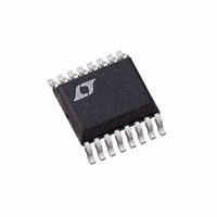
LTC2440IGN#PBF Linear Technology, LTC2440IGN#PBF Datasheet - Page 12

LTC2440IGN#PBF
Manufacturer Part Number
LTC2440IGN#PBF
Description
IC ADC DIFFER 24-BIT HS 16-SSOP
Manufacturer
Linear Technology
Datasheet
1.LTC2440CGN.pdf
(28 pages)
Specifications of LTC2440IGN#PBF
Number Of Bits
24
Sampling Rate (per Second)
3.5k
Data Interface
MICROWIRE™, Serial, SPI™
Number Of Converters
2
Power Dissipation (max)
40mW
Voltage Supply Source
Single Supply
Operating Temperature
-40°C ~ 85°C
Mounting Type
Surface Mount
Package / Case
16-SSOP (0.150", 3.90mm Width)
Lead Free Status / RoHS Status
Lead free / RoHS Compliant
Available stocks
Company
Part Number
Manufacturer
Quantity
Price
Table 2. LTC2440 Output Data Format
Differential Input Voltage
V
V
0.5 • V
0.25 • V
0.25 • V
0
–1LSB
–0.25 • V
–0.25 • V
–0.5 • V
V
*The differential input voltage V
LTC2440
APPLICATIONS INFORMATION
microcontroller. Bit 31 (EOC) can be captured on the fi rst
rising edge of SCK. Bit 30 is shifted out of the device on
the fi rst falling edge of SCK. The fi nal data bit (Bit 0) is
shifted out on the falling edge of the 31st SCK and may
be latched on the rising edge of the 32nd SCK pulse. On
the falling edge of the 32nd SCK pulse, SDO goes HIGH
indicating the initiation of a new conversion cycle. This
bit serves as EOC (Bit 31) for the next conversion cycle.
Table 2 summarizes the output data format.
As long as the voltage on the IN
tained within the –0.3V to (V
operating range, a conversion result is generated for any
differential input voltage V
+FS = 0.5 • V
than +FS, the conversion result is clamped to the value
corresponding to the +FS + 1LSB. For differential input
voltages below –FS, the conversion result is clamped to
the value corresponding to –FS – 1LSB.
SERIAL INTERFACE PINS
The LTC2440 transmits the conversion results and receives
the start of conversion command through a synchronous
2-wire, 3-wire or 4-wire interface. During the conversion
and sleep states, this interface can be used to assess
the converter status and during the data output state it
is used to read the conversion result and program the
speed/resolution.
12
IN
IN
IN
*
* ≥ 0.5 • V
* < –0.5 • V
REF
REF
REF
REF
REF
REF
** – 1LSB
**
** – 1LSB
**
**
** – 1LSB
REF
REF
**
**
REF
. For differential input voltages greater
IN
= IN
IN
CC
Bit 31
EOC
+
from –FS = –0.5 • V
+ 0.3V) absolute maximum
0
0
0
0
0
0
0
0
0
0
– IN
+
–
. **The differential reference voltage V
and IN
Bit 30
DMY
0
0
0
0
0
0
0
0
0
0
–
pins is main-
Bit 29
SIG
1
1
1
1
1
0
0
0
0
0
REF
to
Bit 28
MSB
1
0
0
0
0
1
1
1
1
0
Serial Clock Input/Output (SCK)
The serial clock signal present on SCK (Pin 13) is used to
synchronize the data transfer. Each bit of data is shifted out
the SDO pin on the falling edge of the serial clock.
In the Internal SCK mode of operation, the SCK pin is an
output and the LTC2440 creates its own serial clock. In
the External SCK mode of operation, the SCK pin is used
as input. The internal or external SCK mode is selected
by tying EXT (Pin 10) LOW for external SCK and HIGH
for internal SCK.
Serial Data Output (SDO)
The serial data output pin, SDO (Pin 12), provides the
result of the last conversion as a serial bit stream (MSB
fi rst) during the data output state. In addition, the SDO
pin is used as an end of conversion indicator during the
conversion and sleep states.
When CS (Pin 11) is HIGH, the SDO driver is switched
to a high impedance state. This allows sharing the serial
interface with other devices. If CS is LOW during the
convert or sleep state, SDO will output EOC. If CS is LOW
during the conversion phase, the EOC bit appears HIGH
on the SDO pin. Once the conversion is complete, EOC
goes LOW. The device remains in the sleep state until the
fi rst rising edge of SCK occurs while CS = LOW.
REF
= REF
Bit 27
0
1
1
0
0
1
1
0
0
1
+
– REF
–
.
Bit 26
0
1
0
1
0
1
0
1
0
1
Bit 25
0
1
0
1
0
1
0
1
0
1
…
…
…
…
…
…
…
…
…
…
…
Bit 0
0
1
0
1
0
1
0
1
0
1
2440fd


