LTC2290IUP#PBF Linear Technology, LTC2290IUP#PBF Datasheet - Page 18
LTC2290IUP#PBF
Manufacturer Part Number
LTC2290IUP#PBF
Description
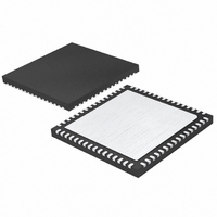
IC ADC DUAL 12BIT 10MSPS 64QFN
Manufacturer
Linear Technology
Datasheet
1.LTC2290CUPPBF.pdf
(24 pages)
Specifications of LTC2290IUP#PBF
Number Of Bits
12
Sampling Rate (per Second)
10M
Data Interface
Parallel
Number Of Converters
2
Power Dissipation (max)
138mW
Voltage Supply Source
Single Supply
Operating Temperature
-40°C ~ 85°C
Mounting Type
Surface Mount
Package / Case
64-WFQFN, Exposed Pad
Lead Free Status / RoHS Status
Lead free / RoHS Compliant


LTC2290
APPLICATIO S I FOR ATIO
Digital Output Multiplexer
The digital outputs of the LTC2290 can be multiplexed onto
a single data bus. The MUX pin is a digital input that swaps
the two data busses. If MUX is High, Channel A comes out
on DA0-DA11, OFA; Channel B comes out on DB0-DB11,
OFB. If MUX is Low, the output busses are swapped and
Channel A comes out on DB0-DB11, OFB; Channel B comes
out on DA0-DA11, OFA. To multiplex both channels onto
a single output bus, connect MUX, CLKA and CLKB together
(see the Timing Diagram for the multiplexed mode). The
multiplexed data is available on either data bus—the un-
used data bus can be disabled with its OE pin.
Grounding and Bypassing
The LTC2290 requires a printed circuit board with a clean,
unbroken ground plane. A multilayer board with an inter-
nal ground plane is recommended. Layout for the printed
circuit board should ensure that digital and analog signal
lines are separated as much as possible. In particular, care
should be taken not to run any digital track alongside an
analog signal track or underneath the ADC.
18
U
U
W
U
High quality ceramic bypass capacitors should be used
at the V
capacitors must be located as close to the pins as possible.
Of particular importance is the 0.1µF capacitor between
REFH and REFL. This capacitor should be placed as close
to the device as possible (1.5mm or less). A size 0402
ceramic capacitor is recommended. The large 2.2µF
capacitor between REFH and REFL can be somewhat
further away. The traces connecting the pins and bypass
capacitors must be kept short and should be made as wide
as possible.
The LTC2290 differential inputs should run parallel and
close to each other. The input traces should be as short as
possible to minimize capacitance and to minimize noise
pickup.
Heat Transfer
Most of the heat generated by the LTC2290 is transferred
from the die through the bottom-side exposed pad and
package leads onto the printed circuit board. For good
electrical and thermal performance, the exposed pad
should be soldered to a large grounded pad on the PC
board. It is critical that all ground pins are connected to a
ground plane of sufficient area.
DD
, OV
DD
, V
CM
, REFH, and REFL pins. Bypass
2290fa
Related parts for LTC2290IUP#PBF
Image
Part Number
Description
Manufacturer
Datasheet
Request
R

Part Number:
Description:
CD ROM LINEARVIEW DATASHEETS
Manufacturer:
Linear Technology

Part Number:
Description:
Standalone Linear Li-Ion Battery Charger with Thermal Regulation in ThinSOT
Manufacturer:
Linear Technology Corporation
Datasheet:
Part Number:
Description:
Low noise, high frequency, 8th order linear phase lowpass filter
Manufacturer:
Linear Technology Corporation
Datasheet:
Part Number:
Description:
Manufacturer:
Linear Technology Corporation
Datasheet:
Part Number:
Description:
Manufacturer:
Linear Technology Corporation
Datasheet:
Part Number:
Description:
Manufacturer:
Linear Technology Corporation
Datasheet:
Part Number:
Description:
Manufacturer:
Linear Technology Corporation
Datasheet:
Part Number:
Description:
Manufacturer:
Linear Technology Corporation
Datasheet:
Part Number:
Description:
Manufacturer:
Linear Technology Corporation
Datasheet:
Part Number:
Description:
Manufacturer:
Linear Technology Corporation
Datasheet:
Part Number:
Description:
Dual and Quad, JFET Input Precision High Speed Op Amps
Manufacturer:
Linear Technology Corporation
Datasheet:
Part Number:
Description:
Manufacturer:
Linear Technology Corporation
Datasheet:
Part Number:
Description:
1, 2, 6 and 8 Channel, 10-Bit Serial I/O Data Acquisition Systems
Manufacturer:
Linear Technology Corporation
Datasheet:
Part Number:
Description:
Manufacturer:
Linear Technology Corporation
Datasheet:
Part Number:
Description:
Universal dual filter building block
Manufacturer:
Linear Technology Corporation
Datasheet: