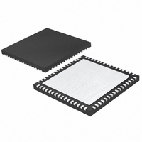
LTC2290IUP#PBF Linear Technology, LTC2290IUP#PBF Datasheet - Page 5

LTC2290IUP#PBF
Manufacturer Part Number
LTC2290IUP#PBF
Description
IC ADC DUAL 12BIT 10MSPS 64QFN
Manufacturer
Linear Technology
Datasheet
1.LTC2290CUPPBF.pdf
(24 pages)
Specifications of LTC2290IUP#PBF
Number Of Bits
12
Sampling Rate (per Second)
10M
Data Interface
Parallel
Number Of Converters
2
Power Dissipation (max)
138mW
Voltage Supply Source
Single Supply
Operating Temperature
-40°C ~ 85°C
Mounting Type
Surface Mount
Package / Case
64-WFQFN, Exposed Pad
Lead Free Status / RoHS Status
Lead free / RoHS Compliant
POWER REQUIRE E TS
SYMBOL
V
OV
IV
P
P
P
range, otherwise specifications are at T
range, otherwise specifications are at T
SYMBOL
f
t
t
t
t
t
Pipeline Latency
Note 1: Stresses beyond those listed under Absolute Maximum Ratings
may cause permanent damage to the device. Exposure to any Absolute
Maximum Rating condition for extended periods may affect device
reliability and lifetime.
Note 2: All voltage values are with respect to ground with GND and OGND
wired together (unless otherwise noted).
Note 3: When these pin voltages are taken below GND or above V
will be clamped by internal diodes. This product can handle input currents
of greater than 100mA below GND or above V
Note 4: V
drive, unless otherwise noted.
TI I G CHARACTERISTICS
s
L
H
AP
D
MD
DD
DISS
SHDN
NAP
DD
DD
W
DD
U
= 3V, f
SAMPLE
PARAMETER
Analog Supply Voltage
Output Supply Voltage
Supply Current
Power Dissipation
Shutdown Power (Each Channel)
Nap Mode Power (Each Channel)
PARAMETER
Sampling Frequency
CLK Low Time
CLK High Time
Sample-and-Hold Aperture Delay
CLK to DATA Delay
MUX to DATA Delay
Data Access Time After OE↓
BUS Relinquish Time
= 10MHz, input range = 2V
W U
A
A
DD
= 25°C. (Note 8)
= 25°C. (Note 4)
without latchup.
P-P
The
with differential
The
●
denotes the specifications which apply over the full operating temperature
●
DD
denotes the specifications which apply over the full operating temperature
, they
CONDITIONS
(Note 9)
(Note 9)
Both ADCs at f
Both ADCs at f
SHDN = H, OE = H, No CLK
SHDN = H, OE = L, No CLK
CONDITIONS
(Note 9)
Duty Cycle Stabilizer Off
Duty Cycle Stabilizer On (Note 7)
Duty Cycle Stabilizer Off
Duty Cycle Stabilizer On (Note 7)
C
C
C
(Note 7)
L
L
L
= 5pF (Note 7)
= 5pF (Note 7)
= 5pF (Note 7)
Note 5: Integral nonlinearity is defined as the deviation of a code from a
straight line passing through the actual endpoints of the transfer curve.
The deviation is measured from the center of the quantization band.
Note 6: Offset error is the offset voltage measured from –0.5 LSB when
the output code flickers between 0000 0000 0000 and 1111 1111 1111.
Note 7: Guaranteed by design, not subject to test.
Note 8: V
drive. The supply current and power dissipation are the sum total for both
channels with both channels active.
Note 9: Recommended operating conditions.
S(MAX)
S(MAX)
DD
= 3V, f
SAMPLE
= 10MHz, input range = 1V
●
●
●
●
●
●
●
●
●
●
●
●
●
MIN
MIN
2.7
0.5
1.4
1.4
40
40
1
5
5
TYP
120
TYP
2.7
2.7
4.3
3.3
40
15
50
50
50
50
3
3
2
0
5
LTC2290
P-P
with differential
MAX
MAX
138
500
500
500
500
3.4
3.6
5.4
5.4
8.5
46
10
10
UNITS
UNITS
Cycles
2290fa
5
MHz
mW
mW
mW
mA
nS
ns
ns
ns
ns
ns
ns
ns
ns
V
V


