LTC2290IUP#PBF Linear Technology, LTC2290IUP#PBF Datasheet - Page 8
LTC2290IUP#PBF
Manufacturer Part Number
LTC2290IUP#PBF
Description
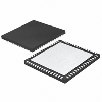
IC ADC DUAL 12BIT 10MSPS 64QFN
Manufacturer
Linear Technology
Datasheet
1.LTC2290CUPPBF.pdf
(24 pages)
Specifications of LTC2290IUP#PBF
Number Of Bits
12
Sampling Rate (per Second)
10M
Data Interface
Parallel
Number Of Converters
2
Power Dissipation (max)
138mW
Voltage Supply Source
Single Supply
Operating Temperature
-40°C ~ 85°C
Mounting Type
Surface Mount
Package / Case
64-WFQFN, Exposed Pad
Lead Free Status / RoHS Status
Lead free / RoHS Compliant


PI FU CTIO S
LTC2290
A
Input.
A
Input.
REFHA (Pins 3, 4): Channel A High Reference. Short
together and bypass to Pins 5, 6 with a 0.1µF ceramic chip
capacitor as close to the pin as possible. Also bypass to
Pins 5, 6 with an additional 2.2µF ceramic chip capacitor
and to ground with a 1µF ceramic chip capacitor.
REFLA (Pins 5, 6): Channel A Low Reference. Short
together and bypass to Pins 3, 4 with a 0.1µF ceramic chip
capacitor as close to the pin as possible. Also bypass to
Pins 3, 4 with an additional 2.2µF ceramic chip capacitor
and to ground with a 1µF ceramic chip capacitor.
V
GND with 0.1µF ceramic chip capacitors.
CLKA (Pin 8): Channel A Clock Input. The input sample
starts on the positive edge.
CLKB (Pin 9): Channel B Clock Input. The input sample
starts on the positive edge.
REFLB (Pins 11, 12): Channel B Low Reference. Short
together and bypass to Pins 13, 14 with a 0.1µF ceramic
chip capacitor as close to the pin as possible. Also bypass
to Pins 13, 14 with an additional 2.2µF ceramic chip ca-
pacitor and to ground with a 1µF ceramic chip capacitor.
REFHB (Pins 13, 14): Channel B High Reference. Short
together and bypass to Pins 11, 12 with a 0.1µF ceramic
chip capacitor as close to the pin as possible. Also bypass
to Pins 11, 12 with an additional 2.2µF ceramic chip ca-
pacitor and to ground with a 1µF ceramic chip capacitor.
A
Input.
A
Input.
GND (Pins 17, 64): ADC Power Ground.
SENSEB (Pin 19): Channel B Reference Programming Pin.
Connecting SENSEB to V
and a ±0.5V input range. V
8
INA
INA
DD
INB
INB
U
+
–
–
+
(Pins 7, 10, 18, 63): Analog 3V Supply. Bypass to
(Pin 15): Channel B Negative Differential Analog
(Pin 2): Channel A Negative Differential Analog
(Pin 16): Channel B Positive Differential Analog
(Pin 1): Channel A Positive Differential Analog
U
U
CMB
DD
selects the internal reference
selects the internal reference
and a ±1V input range. An external reference greater than
0.5V and less than 1V applied to SENSEB selects an input
range of ±V
V
Mode Bias. Bypass to ground with 2.2µF ceramic chip
capacitor. Do not connect to V
MUX (Pin 21): Digital Output Multiplexer Control. If MUX
is High, Channel A comes out on DA0-DA11, OFA; Channel B
comes out on DB0-DB11, OFB. If MUX is Low, the output
busses are swapped and Channel A comes out on DB0-
DB11, OFB; Channel B comes out on DA0-DA11, OFA. To
multiplex both channels onto a single output bus, connect
MUX, CLKA and CLKB together.
SHDNB (Pin 22): Channel B Shutdown Mode Selection
Pin. Connecting SHDNB to GND and OEB to GND results
in normal operation with the outputs enabled. Connecting
SHDNB to GND and OEB to V
tion with the outputs at high impedance. Connecting
SHDNB to V
the outputs at high impedance. Connecting SHDNB to V
and OEB to V
high impedance.
OEB (Pin 23): Channel B Output Enable Pin. Refer to
SHDNB pin function.
NC (Pins 24, 25, 41, 42): Do Not Connect These Pins.
DB0 – DB11 (Pins 26 to 30, 33 to 39): Channel B Digital
Outputs. DB11 is the MSB.
OGND (Pins 31, 50): Output Driver Ground.
OV
ers. Bypass to ground with 0.1µF ceramic chip capacitor.
OFB (Pin 40): Channel B Overflow/Underflow Output.
High when an overflow or underflow has occurred.
DA0 – DA11 (Pins 43 to 48, 51 to 56): Channel A Digital
Outputs. DA11 is the MSB.
OFA (Pin 57): Channel A Overflow/Underflow Output.
High when an overflow or underflow has occurred.
OEA (Pin 58): Channel A Output Enable Pin. Refer to
SHDNA Pin Function.
CMB
DD
(Pin 20): Channel B 1.5V Output and Input Common
(Pins 32, 49): Positive Supply for the Output Driv-
SENSEB
DD
DD
and OEB to GND results in nap mode with
results in sleep mode with the outputs at
. ±1V is the largest valid input range.
DD
CMA
results in normal opera-
.
2290fa
DD
Related parts for LTC2290IUP#PBF
Image
Part Number
Description
Manufacturer
Datasheet
Request
R

Part Number:
Description:
CD ROM LINEARVIEW DATASHEETS
Manufacturer:
Linear Technology

Part Number:
Description:
Standalone Linear Li-Ion Battery Charger with Thermal Regulation in ThinSOT
Manufacturer:
Linear Technology Corporation
Datasheet:
Part Number:
Description:
Low noise, high frequency, 8th order linear phase lowpass filter
Manufacturer:
Linear Technology Corporation
Datasheet:
Part Number:
Description:
Manufacturer:
Linear Technology Corporation
Datasheet:
Part Number:
Description:
Manufacturer:
Linear Technology Corporation
Datasheet:
Part Number:
Description:
Manufacturer:
Linear Technology Corporation
Datasheet:
Part Number:
Description:
Manufacturer:
Linear Technology Corporation
Datasheet:
Part Number:
Description:
Manufacturer:
Linear Technology Corporation
Datasheet:
Part Number:
Description:
Manufacturer:
Linear Technology Corporation
Datasheet:
Part Number:
Description:
Manufacturer:
Linear Technology Corporation
Datasheet:
Part Number:
Description:
Dual and Quad, JFET Input Precision High Speed Op Amps
Manufacturer:
Linear Technology Corporation
Datasheet:
Part Number:
Description:
Manufacturer:
Linear Technology Corporation
Datasheet:
Part Number:
Description:
1, 2, 6 and 8 Channel, 10-Bit Serial I/O Data Acquisition Systems
Manufacturer:
Linear Technology Corporation
Datasheet:
Part Number:
Description:
Manufacturer:
Linear Technology Corporation
Datasheet:
Part Number:
Description:
Universal dual filter building block
Manufacturer:
Linear Technology Corporation
Datasheet: