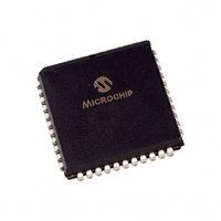
TC850CLW Microchip Technology, TC850CLW Datasheet - Page 11

TC850CLW
Manufacturer Part Number
TC850CLW
Description
IC ADC 15BIT FAST 44PLCC
Manufacturer
Microchip Technology
Datasheet
1.TC850CPL.pdf
(26 pages)
Specifications of TC850CLW
Data Interface
Parallel
Number Of Bits
15
Sampling Rate (per Second)
40
Number Of Converters
1
Voltage Supply Source
Dual ±
Operating Temperature
0°C ~ 70°C
Mounting Type
Surface Mount
Package / Case
44-PLCC
Resolution (bits)
15bit
Sampling Rate
40SPS
Input Channel Type
Differential
Supply Voltage Range - Analog
± 5V
Supply Current
2mA
Digital Ic Case Style
LCC
Lead Free Status / RoHS Status
Lead free / RoHS Compliant
Available stocks
Company
Part Number
Manufacturer
Quantity
Price
Company:
Part Number:
TC850CLW
Manufacturer:
MICROCHIP
Quantity:
12 000
Company:
Part Number:
TC850CLW
Manufacturer:
Microchip Technology
Quantity:
10 000
Part Number:
TC850CLW
Manufacturer:
TELCOM
Quantity:
20 000
Company:
Part Number:
TC850CLW713
Manufacturer:
MICROCHIP
Quantity:
12 000
Company:
Part Number:
TC850CLW713
Manufacturer:
Microchip Technology
Quantity:
10 000
5.0
5.1
The analog signal to be measured is applied at the IN+
and IN– inputs. The differential input voltage must be
within the Common mode range of the converter. The
input Common mode range extends from V
V
an 80 dB CMRR is typical.
The integrator output also follows the Common mode
voltage. The integrator output must not be allowed to
saturate. A worst-case condition exists, for example,
when a large, positive Common mode voltage, with a
near full scale negative differential input voltage, is
applied. The negative input signal drives the integrator
positive when most of its available swing has been
used up by the positive Common mode voltage. For
applications where maximum Common mode range is
critical, integrator swing can be reduced. The integrator
output can swing within 0.4V of either supply without
loss of linearity.
5.2
The TC850 requires two reference voltage sources in
order to generate the “fast-slow” de-integrate phases.
The main voltage reference (V
the REF
(V
The reference voltage inputs are fully differential and
the reference voltage can be generated anywhere
within the power supply voltage of the converter. How-
ever, to minimize rollover error, especially at high con-
version rates, keep the reference Common mode
voltage (i.e., REF-) near or at the analog common
potential. All voltage reference inputs are high-imped-
ance. Average reference input current is typically only
30 pA.
© 2006 Microchip Technology Inc.
SS
REF2
+1.5V. Within this Common mode voltage range,
) is applied between the REF
1
PIN DESCRIPTION (ANALOG)
Differential Inputs (IN+ and IN–)
Differential Reference (V
+ and REF- pins. The secondary reference
REF1
) is applied between
2
+ and REF- pins.
REF
DD
)
- 1.5V to
5.3
Analog common is used as the IN- return during the
zero integrator and de-integrate phases of each con-
version. If IN- is at a different potential than analog
common, a Common mode voltage exists in the sys-
tem. This signal is rejected by the 80dB CMRR of the
converter. However, in most applications, IN- will be set
at a fixed, known voltage (power supply common, for
instance). In this case, analog common should be tied
to the same point so that the Common mode voltage is
eliminated.
Analog Common (ANALOG
COMMON)
DS21479C-page 11
TC850


