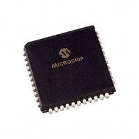
TC850CLW Microchip Technology, TC850CLW Datasheet - Page 2

TC850CLW
Manufacturer Part Number
TC850CLW
Description
IC ADC 15BIT FAST 44PLCC
Manufacturer
Microchip Technology
Datasheet
1.TC850CPL.pdf
(26 pages)
Specifications of TC850CLW
Data Interface
Parallel
Number Of Bits
15
Sampling Rate (per Second)
40
Number Of Converters
1
Voltage Supply Source
Dual ±
Operating Temperature
0°C ~ 70°C
Mounting Type
Surface Mount
Package / Case
44-PLCC
Resolution (bits)
15bit
Sampling Rate
40SPS
Input Channel Type
Differential
Supply Voltage Range - Analog
± 5V
Supply Current
2mA
Digital Ic Case Style
LCC
Lead Free Status / RoHS Status
Lead free / RoHS Compliant
Available stocks
Company
Part Number
Manufacturer
Quantity
Price
Company:
Part Number:
TC850CLW
Manufacturer:
MICROCHIP
Quantity:
12 000
Company:
Part Number:
TC850CLW
Manufacturer:
Microchip Technology
Quantity:
10 000
Part Number:
TC850CLW
Manufacturer:
TELCOM
Quantity:
20 000
Company:
Part Number:
TC850CLW713
Manufacturer:
MICROCHIP
Quantity:
12 000
Company:
Part Number:
TC850CLW713
Manufacturer:
Microchip Technology
Quantity:
10 000
TC850
General Description:
The TC850 is a monolithic CMOS A/D converter (ADC)
with resolution of 15-bits plus sign. It combines a
chopper-stabilized buffer and integrator with a unique
multiple-slope integration technique that increases
conversion speed. The result is 16 times improvement
in speed over previous 15-bit, monolithic integrating
ADCs (from 2.5 conversions per second up to 40 per
second). Faster conversion speed is especially
welcome in systems with human interface, such as
digital scales.
The TC850 incorporates an ADC and a μP-compatible
digital interface. Only a voltage reference and a few,
noncritical, passive components are required to form a
complete 15-bit plus sign ADC. CMOS processing
provides the TC850 with high-impedance, differential
inputs. Input bias current is typically only 30 pA, permit-
ting direct interface to sensors. Input sensitivity of 100
μV per Least Significant bit (LSb) eliminates the need
Functional Block Diagram
DS21479C-page 2
COMMON
IN+
IN-
Pinout of 40-Pin Package
32
31
30
17
OSC
REF
39
Clock
Oscillator
1
Analog
1
REF
34
+
Mux
Sequencer
Control
2
36
A/D
REF-
+
OSC
18
2
÷4
DEMAND
CONT/
-
+
BUF
5
Buffer
25
L/H
7
R
INT IN
INT
OVR/
POL
24
6
TC850
for precision external amplifiers. The internal amplifiers
are auto-zeroed, ensuring a zero digital output, with 0V
analog input. Zero adjustment potentiometers or
calibrations are not required.
The TC850 outputs data on an 8-bit, 3-state bus. Digital
inputs are CMOS compatible while outputs are TTL/
CMOS compatible. Chip-enable and byte-select inputs,
combined with an end-of-conversion output, ensures
easy interfacing to a wide variety of microprocessors.
Conversions can be performed continuously or on
command. In Continuous mode, data is read as three
consecutive bytes and manipulation of address lines is
not required.
Operating from ±5V supplies, the TC850 dissipates
only 20 mΩ. The TC850 is packaged in a 40-pin plastic
or ceramic dual-in-line package (DIPs) and in a 44-pin
plastic leaded chip carrier (PLCC), surface-mount
package.
WR
3
C
Decode Logic
Bus Interface
INT
-
+
INT OUT
4
RD
Integrator
1
CS
23
2
CE
Up/Down
Counter
Octal 2-Input Mux
+
3-State Data Bus
-
6-Bit
© 2006 Microchip Technology Inc.
15
Comparator
22
DB0
–5V
Data Latch
. . . .
Up/Down
Counter
9-Bit
40
DB7
+5V
8


