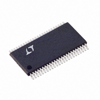
LTC1748CFW#TR Linear Technology, LTC1748CFW#TR Datasheet - Page 14

LTC1748CFW#TR
Manufacturer Part Number
LTC1748CFW#TR
Description
IC ADC SMPL 14BIT 80MSPS 48TSSOP
Manufacturer
Linear Technology
Datasheet
1.LTC1748CFW.pdf
(20 pages)
Specifications of LTC1748CFW#TR
Number Of Bits
14
Sampling Rate (per Second)
80M
Data Interface
Parallel
Number Of Converters
1
Power Dissipation (max)
1.55W
Voltage Supply Source
Single Supply
Operating Temperature
0°C ~ 70°C
Mounting Type
Surface Mount
Package / Case
48-TFSOP (0.240", 6.10mm Width)
Lead Free Status / RoHS Status
Contains lead / RoHS non-compliant
Available stocks
Company
Part Number
Manufacturer
Quantity
Price
APPLICATIO S I FOR ATIO
LTC1748
mode voltage of any external input circuitry; additionally,
the reference is used with a difference amplifier to gener-
ate the differential reference levels needed by the internal
ADC circuitry.
An external bypass capacitor is required for the 2.35V
reference output, V
impedance path to ground for internal and external cir-
cuitry. This is also the compensation capacitor for the
reference. It will not be stable without this capacitor.
The difference amplifier generates the high and low refer-
ence for the ADC. High speed switching circuits are
connected to these outputs and they must be externally
bypassed. Each output has two pins: REFHA and REFHB
for the high reference and REFLA and REFLB for the low
reference. The doubled output pins are needed to reduce
package inductance. Bypass capacitors must be con-
nected as shown in Figure 5.
Other voltage ranges in between the pin selectable ranges
can be programmed with two external resistors as shown
in Figure 6a. An external reference can be used by applying
its output directly or through a resistor divider to SENSE.
It is not recommended to drive the SENSE pin with a logic
device since the logic threshold is close to ground and
TIE TO V
14
TIE TO GND FOR 2V RANGE;
RANGE = 2 • V
DD
1V < V
FOR 3.2V RANGE;
SENSE
SENSE
Figure 5. Equivalent Reference Circuit
2.35V
< 1.6V
1 F
1 F
FOR
CM
U
4.7 F
. This provides a high frequency low
0.1 F
4.7 F
0.1 F
SENSE
REFHA
REFHB
REFLB
REFLA
V
CM
U
LTC1748
CONTROL
DETECT
4
RANGE
AND
W
2.35V BANDGAP
DIFF AMP
REFERENCE
INTERNAL ADC
HIGH REFERENCE
INTERNAL ADC
LOW REFERENCE
1.6V
BUFFER
U
1V
1748 F05
V
the converter as possible. If the SENSE pin is driven
externally, it should be bypassed to ground as close to the
device as possible with a 1 F ceramic capacitor.
Input Range
The input range can be set based on the application. For
oversampled signal processing in which the input fre-
quency is low (<10MHz), the largest input range will
provide the best signal-to-noise performance while main-
taining excellent SFDR. For high input frequencies
(> 40MHz), the 2V range will have the best SFDR perfor-
mance for the 2nd and 3rd harmonics, but the SNR will
degrade by 3.5dB. See the Typical Performance Charac-
teristics section.
Driving the Encode Inputs
The noise performance of the LTC1748 can depend on the
encode signal quality as much as on the analog input. The
ENC/ENC inputs are intended to be driven differentially,
primarily for noise immunity from common mode noise
sources. Each input is biased through a 6k resistor to a 2V
bias. The bias resistors set the DC operating point for
transformer coupled drive circuits and can set the logic
threshold for single-ended drive circuits.
DD
. The SENSE pin should be tied high or low as close to
Figure 6b. 2.5V Range ADC with External Reference
5V
0.1 F
Figure 6a. 2.2V Range ADC
4
12.5k
11k
2.35V
LT1790-1.25
1.1V
1, 2
SENSE
4.7 F
1 F
V
6
CM
2.35V
1.25V
LTC1748
1748 F06a
SENSE
4.7 F
1 F
V
CM
LTC1748
1748 F06b
1748fa


