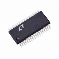
LTC1604ACG#PBF Linear Technology, LTC1604ACG#PBF Datasheet - Page 6

LTC1604ACG#PBF
Manufacturer Part Number
LTC1604ACG#PBF
Description
IC A/D CONV 16BIT SAMPLNG 36SSOP
Manufacturer
Linear Technology
Datasheet
1.LTC1604CGPBF.pdf
(20 pages)
Specifications of LTC1604ACG#PBF
Number Of Bits
16
Sampling Rate (per Second)
333k
Data Interface
Parallel
Number Of Converters
1
Power Dissipation (max)
350mW
Voltage Supply Source
Dual ±
Operating Temperature
0°C ~ 70°C
Mounting Type
Surface Mount
Package / Case
36-SSOP (0.200", 5.30mm Width)
Lead Free Status / RoHS Status
Lead free / RoHS Compliant
Available stocks
Company
Part Number
Manufacturer
Quantity
Price
LTC1604
PIN
A
difference voltage between A
tial range of 2.5V. A
A
A
to a DC voltage or driven differentially with A
V
2.2 F tantalum in parallel with 0.1 F ceramic.
REFCOMP (Pin 4): 4.375 Reference Compensation Pin.
Bypass to AGND with 47 F tantalum in parallel with 0.1 F
ceramic.
AGND (Pins 5 to 8): Analog Grounds. Tie to analog ground
plane.
DV
with 10 F tantalum in parallel with 0.1 F ceramic.
DGND (Pin 10): Digital Ground for Internal Logic. Tie to
analog ground plane.
D15 to D0 (Pins 11 to 26): Three-State Data Outputs. D15
is the Most Significant Bit.
BUSY (Pin 27): The BUSY output shows the converter
status. It is low when a conversion is in progress. Data is
valid on the rising edge of BUSY.
6
TYPICAL PERFORMANCE CHARACTERISTICS
–100
–120
–140
IN
IN
IN
REF
–20
–40
–60
–80
DD
U
+
–
–
0
(Pin 2): Negative Analog Input. Can be grounded, tied
0
(Pin 1): Positive Analog Input. The ADC converts the
is grounded.
(Pin 3): 2.5V Reference Output. Bypass to AGND with
Intermodulaton Distortion
(Pin 9): 5V Digital Power Supply. Bypass to DGND
FUNCTIONS
20
U
40
FREQUENCY (kHz)
60
80 100
U
IN
f
f
f
SAMPLE
IN1
IN2
+
= 29.3kHz
= 32.4kHz
120 140
has a 2.5V input range when
W
= 333kHz
IN
+
1604 G06
and A
160
U
IN
–
with a differen-
–100
–120
–20
–40
–60
–80
0
IN
1k
Power Supply Feedthrough vs
Ripple Frequency
+
f
V
SAMPLE
.
RIPPLE
= 10mV
= 333kHz
INPUT FREQUENCY (Hz)
10k
A
V
VDD
SS
OGND (Pin 28): Digital Ground for Output Drivers.
OV
Bypass to OGND with 10 F tantalum in parallel with 0.1 F
ceramic.
RD (Pin 30): Read Input. A logic low enables the output
drivers when CS is low.
CONVST (Pin 31): Conversion Start Signal. This active
low signal starts a conversion on its falling edge when CS
is low.
CS (Pin 32): The Chip Select Input. Must be low for the
ADC to recognize CONVST and RD inputs.
SHDN (Pin 33): Power Shutdown. Drive this pin low with
CS low for nap mode. Drive this pin low with CS high for
sleep mode.
V
10 F tantalum in parallel with 0.1 F ceramic.
AV
with 10 F tantalum in parallel with 0.1 F ceramic.
AV
with 10 F tantalum in parallel with 0.1 F ceramic and
connect this pin to Pin 35 with a 10 resistor.
SS
DD
DD
DD
100k
(Pin 34): – 5V Negative Supply. Bypass to AGND with
(Pin 35): 5V Analog Power Supply. Bypass to AGND
(Pin 36): 5V Analog Power Supply. Bypass to AGND
(Pin 29): Digital Power Supply for Output Drivers.
1604 G07
1M
80
70
60
50
40
30
20
10
0
1k
Input Common Mode Rejection
vs Input Frequency
INPUT FREQUENCY (Hz)
10k
100k
1604G09
1M


