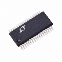
LTC1604ACG#PBF Linear Technology, LTC1604ACG#PBF Datasheet

LTC1604ACG#PBF
Specifications of LTC1604ACG#PBF
Available stocks
Related parts for LTC1604ACG#PBF
LTC1604ACG#PBF Summary of contents
Page 1
... The ADC has P compatible,16-bit parallel output port. There is no pipeline delay in conversion results. A separate convert start input and a data ready signal (BUSY) ease connections to FlFOs, DSPs and microprocessors. , LTC and LT are registered trademarks of Linear Technology Corporation ...
Page 2
LTC1604 ABSOLUTE MAXIMUM (Notes Supply Voltage (V ) ................................................ 6V DD Negative Supply Voltage (V )................................ – Total Supply Voltage (V to ...
Page 3
ACCURACY SYMBOL PARAMETER S/N Signal-to-Noise Ratio S/( Signal-to-(Noise + Distortion) Ratio THD Total Harmonic Distortion Up to 5th Harmonic SFDR Spurious Free Dynamic Range IMD Intermodulation Distortion Full Power Bandwidth Full Linear Bandwidth ...
Page 4
LTC1604 W U POWER REQUIRE E TS SYMBOL PARAMETER V Positive Supply Voltage DD V Negative Supply Voltage SS I Positive Supply Current DD Nap Mode Sleep Mode I Negative Supply Current SS Nap Mode Sleep Mode P Power Dissipation ...
Page 5
CHARACTERISTICS The denotes specifications that apply over the full operating temperature range. Note 1: Absolute Maximum Ratings are those values beyond which the life of a device may be impaired. Note 2: All voltage values ...
Page 6
LTC1604 W U TYPICAL PERFORMANCE CHARACTERISTICS Intermodulaton Distortion 333kHz SAMPLE f = 29.3kHz –20 IN1 f = 32.4kHz IN2 –40 –60 –80 –100 –120 –140 100 120 140 160 FREQUENCY (kHz) 1604 ...
Page 7
CTIO AL BLOCK DIAGRA 2 REF REFCOMP 4 + 4.375V DIFFERENTIAL ANALOG INPUT – 2.5V IN TEST CIRCUITS Load Circuits for Access Timing ...
Page 8
LTC1604 U U APPLICATIONS INFORMATION CONVERSION DETAILS The LTC1604 uses a successive approximation algorithm and internal sample-and-hold circuit to convert an analog signal to a 16-bit parallel output. The ADC is complete with a sample-and-hold, a precision reference and an ...
Page 9
U U APPLICATIONS INFORMATION SHDN Figure 2a. Nap Mode to Sleep Mode Timing SHDN t 4 CONVST Figure 2b. SHDN to CONVST Wake-Up Timing CONVST Figure 3. CS top CONVST Setup ...
Page 10
LTC1604 U U APPLICATIONS INFORMATION CONVST t 6 BUSY DATA (N – 1) DATA D15 TO D0 Figure 5. Mode 1a. CONVST Starts a Conversion. Data Outputs Always Enabled (CONVST = CS = ...
Page 11
U U APPLICATIONS INFORMATION CONVST t 6 BUSY t 10 DATA (N – 1) DATA CONVST t 6 BUSY t 10 DATA three-state until read by the MPU with the ...
Page 12
... DC accuracy and settling time are most critical. The following list is a summary of the op amps that are suitable for driving the LTC1604. More detailed informa- tion is available in the Linear Technology databooks, the TM LinearView CD-ROM and on our web site at: www ...
Page 13
U U APPLICATIONS INFORMATION 100 1 ANALOG INPUT A IN 3000pF REF 4 REFCOMP AGND Figure 11. RC Input Filter Input Range The 2.5V input range of the LTC1604 is optimized for ...
Page 14
LTC1604 U U APPLICATIONS INFORMATION ANALOG INPUT 2V TO 2.7V DIFFERENTIAL 2V TO 2.7V LTC1450 47 F Figure 13. Driving V with a DAC REF 10k 100k INPUT FREQUENCY (Hz) ...
Page 15
U U APPLICATIONS INFORMATION –5V ANALOG INPUT R3 24k R8 50k R4 100 R5 R7 47k 50k R6 24k + 0 Figure 15b. Offset and Full-Scale Adjust Circuit + – (i.e., – 0.5LSB ...
Page 16
LTC1604 U U APPLICATIONS INFORMATION – REF ANALOG INPUT – CIRCUITRY 2 PERFORMANCE The noise of an ADC can be evaluated in two ways: signal- to-noise raio (SNR) ...
Page 17
U U APPLICATIONS INFORMATION Signal-to-Noise Ratio The signal-to-noise plus distortion ratio [S/(N + D)] is the ratio between the RMS amplitude of the fundamental input frequency to the RMS amplitude of all other frequency components at the A/D output. The ...
Page 18
LTC1604 U U APPLICATIONS INFORMATION Intermodulation Distortion If the ADC input signal consists of more than one spectral component, the ADC transfer function nonlinearity can produce intermodulation distortion (IMD) in addition to THD. IMD is the change in one sinusoidal ...
Page 19
... FLASH SHALL NOT EXCEED 0.010" (0.254mm) PER SIDE Information furnished by Linear Technology Corporation is believed to be accurate and reliable. However, no responsibility is assumed for its use. Linear Technology Corporation makes no represen- tation that the interconnection of its circuits as described herein will not infringe on existing patent rights. ...
Page 20
... Low Power, Low Gritch, 4-Quadrant Multiplication DGND DD DD SHDN CONTROL P LOGIC CONVST 31 CONTROL AND 2. LINES TIMING REF BUSY OGND 28 OUTPUT 16-BIT BUFFERS D15 TO D0 PARALLEL BUS AGND –5V 1604fa LT/TP 1098 REV A 2K • PRINTED IN USA LINEAR TECHNOLOGY CORPORATION 1998 1604 TA03 ...


