LTC2220CUP-1#TRPBF Linear Technology, LTC2220CUP-1#TRPBF Datasheet - Page 14

LTC2220CUP-1#TRPBF
Manufacturer Part Number
LTC2220CUP-1#TRPBF
Description
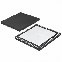
IC ADC 12BIT 185MSPS 64-QFN
Manufacturer
Linear Technology
Datasheet
1.LTC2220CUP-1TRPBF.pdf
(28 pages)
Specifications of LTC2220CUP-1#TRPBF
Number Of Bits
12
Sampling Rate (per Second)
185M
Data Interface
Parallel
Number Of Converters
1
Power Dissipation (max)
1.18W
Voltage Supply Source
Single Supply
Operating Temperature
0°C ~ 70°C
Mounting Type
Surface Mount
Package / Case
64-WFQFN, Exposed Pad
Lead Free Status / RoHS Status
Lead free / RoHS Compliant
Available stocks
Company
Part Number
Manufacturer
Quantity
Price
14
LTC2220-1
DYNAMIC PERFORMANCE
Signal-to-Noise Plus Distortion Ratio
The signal-to-noise plus distortion ratio [S/(N + D)] is the
ratio between the RMS amplitude of the fundamental input
frequency and the RMS amplitude of all other frequency
components at the ADC output. The output is band limited
to frequencies above DC to below half the sampling
frequency.
Signal-to-Noise Ratio
The signal-to-noise ratio (SNR) is the ratio between the
RMS amplitude of the fundamental input frequency and
the RMS amplitude of all other frequency components
except the first five harmonics and DC.
Total Harmonic Distortion
Total harmonic distortion is the ratio of the RMS sum of all
harmonics of the input signal to the fundamental itself. The
out-of-band harmonics alias into the frequency band
between DC and half the sampling frequency. THD is
expressed as:
where V1 is the RMS amplitude of the fundamental fre-
quency and V2 through Vn are the amplitudes of the
second through nth harmonics. The THD calculated in this
data sheet uses all the harmonics up to the fifth.
Intermodulation Distortion
If the ADC input signal consists of more than one spectral
component, the ADC transfer function nonlinearity can
produce intermodulation distortion (IMD) in addition to
THD. IMD is the change in one sinusoidal input caused by
the presence of another sinusoidal input at a different
frequency.
If two pure sine waves of frequencies fa and fb are applied
to the ADC input, nonlinearities in the ADC transfer func-
tion can create distortion products at the sum and differ-
ence frequencies of mfa ± nfb, where m and n = 0, 1, 2, 3,
etc. The 3rd order intermodulation products are 2fa + fb,
2fb + fa, 2fa – fb and 2fb – fa. The intermodulation
distortion is defined as the ratio of the RMS value of either
APPLICATIO S I FOR ATIO
THD = 20Log (√(V2
U
2
+ V3
U
2
+ V4
2
W
+ . . . Vn
2
)/V1)
U
input tone to the RMS value of the largest 3rd order
intermodulation product.
Spurious Free Dynamic Range (SFDR)
Spurious free dynamic range is the peak harmonic or
spurious noise that is the largest spectral component
excluding the input signal and DC. This value is expressed
in decibels relative to the RMS value of a full scale input
signal.
Full Power Bandwidth
The full power bandwidth is that input frequency at which
the amplitude of the reconstructed fundamental is re-
duced by 3dB for a full scale input signal.
Aperture Delay Time
The time from when a rising ENC
to the instant that the input signal is held by the sample and
hold circuit.
Aperture Delay Jitter
The variation in the aperture delay time from conversion to
conversion. This random variation will result in noise
when sampling an AC input. The signal to noise ratio due
to the jitter alone will be:
SNR
CONVERTER OPERATION
As shown in Figure 1, the LTC2220-1 is a CMOS pipelined
multistep converter. The converter has five pipelined ADC
stages; a sampled analog input will result in a digitized
value five cycles later (see the Timing Diagram section).
For optimal AC performance the analog inputs should be
driven differentially. For cost sensitive applications, the
analog inputs can be driven single-ended with slightly
worse harmonic distortion. The encode input is differen-
tial for improved common mode noise immunity. The
LTC2220-1 has two phases of operation, determined by
the state of the differential ENC
brevity, the text will refer to ENC
high and ENC
JITTER
= –20log (2π • f
+
less than ENC
IN
• t
–
+
as ENC low.
JITTER
+
greater than ENC
equals the ENC
+
/ENC
)
–
input pins. For
–
–
voltage
as ENC
2220_1fa


