AD7466BRTZ-R2 Analog Devices Inc, AD7466BRTZ-R2 Datasheet - Page 3
AD7466BRTZ-R2
Manufacturer Part Number
AD7466BRTZ-R2
Description
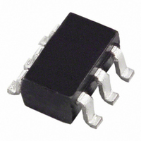
IC ADC 12BIT 1.6V LP SOT23-6
Manufacturer
Analog Devices Inc
Specifications of AD7466BRTZ-R2
Data Interface
DSP, MICROWIRE™, QSPI™, Serial, SPI™
Design Resources
Software Calibrated, 50 MHz to 9 GHz, RF Power Measurement System (CN0178)
Number Of Bits
12
Sampling Rate (per Second)
200k
Number Of Converters
1
Power Dissipation (max)
900µW
Voltage Supply Source
Single Supply
Operating Temperature
-40°C ~ 85°C
Mounting Type
Surface Mount
Package / Case
SOT-23-6
Resolution (bits)
12bit
Sampling Rate
200kSPS
Input Channel Type
Single Ended
Supply Voltage Range - Analog
1.6V To 3.6V
Supply Current
300µA
Lead Free Status / RoHS Status
Lead free / RoHS Compliant
For Use With
EVAL-AD7466CBZ - BOARD EVALUATION FOR AD7466
Lead Free Status / RoHS Status
Lead free / RoHS Compliant, Lead free / RoHS Compliant
Available stocks
Company
Part Number
Manufacturer
Quantity
Price

Part Number:
AD7466BRTZ-R2
Manufacturer:
ADI/亚德诺
Quantity:
20 000


SPECIFICATIONS
AD7466
V
The temperature range for the B version is −40°C to +85°C.
Table 1.
Parameter
DYNAMIC PERFORMANCE
DC ACCURACY
ANALOG INPUT
LOGIC INPUTS
DD
Signal-to-Noise and Distortion (SINAD)
Signal-to-Noise Ratio (SNR)
Total Harmonic Distortion (THD)
Peak Harmonic or Spurious Noise (SFDR)
Intermodulation Distortion (IMD)
Aperture Delay
Aperture Jitter
Full Power Bandwidth
Resolution
Integral Nonlinearity
Differential Nonlinearity
Offset Error
Gain Error
Total Unadjusted Error (TUE)
Input Voltage Ranges
DC Leakage Current
Input Capacitance
Input High Voltage, V
Input Low Voltage, V
Input Current, I
Input Current, I
Input Capacitance, C
= 1.6 V to 3.6 V, f
Second-Order Terms
Third-Order Terms
IN
IN
, SCLK Pin
, CS Pin
SCLK
INL
IN
INH
= 3.4 MHz, f
SAMPLE
= 100 kSPS, unless otherwise noted. T
B Version
69
70
70
70
71
71
70.5
−83
−85
−84
−86
10
40
1.9
750
450
12
−0.9/+1.5
±1
±1
±2
0 to V
±1
20
0.7 × V
2
0.2 × V
0.3 × V
0.8
±1
±1
10
3.2
±1.5
DD
DD
DD
DD
Rev. C | Page 3 of 28
Unit
dB min
dB min
dB typ
dB min
dB typ
dB min
dB typ
dB typ
dB typ
dB typ
dB typ
ns typ
ps typ
MHz typ
MHz typ
kHz typ
kHz typ
Bits
LSB max
LSB max
LSB max
LSB max
LSB max
V
μA max
pF typ
V min
V min
V max
V max
V max
μA max
μA typ
pF max
A
Test Conditions/Comments
f
1.8 V ≤ V
2.5 V ≤ V
V
1.8 V ≤ V
1.8 V ≤ V
2.5 V ≤ V
V
See the Terminology section
See the Terminology section
fa = 29.1 kHz, fb = 29.9 kHz; see the Terminology
section
@ 3 dB, 2.5 V ≤ V
@ 3 dB, 1.6 V ≤ V
@ 0.1 dB, 2.5 V ≤ V
@ 0.1 dB, 1.6 V ≤ V
Maximum specifications apply as typical figures when
V
See the Terminology section
Guaranteed no missed codes to 12 bits; see the
Terminology section
See the Terminology section
See the Terminology section
See the Terminology section
1.6 V ≤ V
2.7 V ≤ V
1.6 V ≤ V
1.8 V ≤ V
2.7 V ≤ V
Typically 20 nA, V
Sample tested at 25°C to ensure compliance
= T
IN
DD
DD
DD
= 30 kHz sine wave
= 1.6 V
= 1.6 V
= 1.6 V
MIN
to T
DD
DD
DD
DD
DD
DD
DD
DD
DD
DD
≤ 2 V; see the Terminology section
≤ 3.6 V
≤ 2 V; see the Terminology section
≤ 2 V
≤ 3.6 V
< 2.7 V
≤ 3.6 V
< 1.8 V
< 2.7 V
≤ 3.6 V
MAX
, unless otherwise noted.
AD7466/AD7467/AD7468
DD
DD
IN
DD
DD
≤ 3.6 V
≤ 2.2 V
= 0 V or V
≤ 3.6 V
≤ 2.2 V
DD
Related parts for AD7466BRTZ-R2
Image
Part Number
Description
Manufacturer
Datasheet
Request
R

Part Number:
Description:
Dual Precision, 500 ns Settling, BiFET Op Amp
Manufacturer:
Analog Devices
Datasheet:

Part Number:
Description:
±1.7g Dual-Axis IMEMS Accelerometer Evaluation Board
Manufacturer:
Analog Devices Inc
Datasheet:

Part Number:
Description:
Inertial Sensor Evaluation System
Manufacturer:
Analog Devices Inc
Datasheet:
Part Number:
Description:
Manufacturer:
Analog Devices Inc
Datasheet:
Part Number:
Description:
Manufacturer:
Analog Devices Inc
Datasheet:
Part Number:
Description:
Manufacturer:
Analog Devices Inc
Datasheet:
Part Number:
Description:
Manufacturer:
Analog Devices Inc
Datasheet:
Part Number:
Description:
Manufacturer:
Analog Devices Inc
Datasheet:
Part Number:
Description:
Manufacturer:
Analog Devices Inc
Datasheet:
Part Number:
Description:
Manufacturer:
Analog Devices Inc
Datasheet:
Part Number:
Description:
Manufacturer:
Analog Devices Inc
Datasheet:
Part Number:
Description:
Manufacturer:
Analog Devices Inc
Datasheet:
Part Number:
Description:
Manufacturer:
Analog Devices Inc
Datasheet: