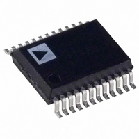
AD7853LARSZ Analog Devices Inc, AD7853LARSZ Datasheet - Page 17

AD7853LARSZ
Manufacturer Part Number
AD7853LARSZ
Description
IC ADC 12BIT SRL 200KSPS 24SSOP
Manufacturer
Analog Devices Inc
Datasheet
1.AD7853LARSZ-REEL.pdf
(34 pages)
Specifications of AD7853LARSZ
Data Interface
8051, QSPI™, Serial, SPI™ µP
Number Of Bits
12
Sampling Rate (per Second)
100k
Number Of Converters
2
Power Dissipation (max)
33mW
Voltage Supply Source
Analog and Digital
Operating Temperature
-40°C ~ 85°C
Mounting Type
Surface Mount
Package / Case
24-SSOP (0.200", 5.30mm Width)
Resolution (bits)
12bit
Sampling Rate
100kSPS
Input Channel Type
Single Ended
Supply Voltage Range - Analog
3V To 5.5V
Supply Voltage Range - Digital
3V To 5.5V
Lead Free Status / RoHS Status
Lead free / RoHS Compliant
REV. B
REFERENCE SECTION
For specified performance, it is recommended that when using
an external reference this reference should be between 2.3 V
and the analog supply AV
reference pins are shown in the typical connection diagrams. If
the internal reference is being used, the REF
should have a 100 nF capacitor connected to AGND very close
to the REF
Figure 18.
If the internal reference is required for use external to the ADC,
it should be buffered at the REF
connected from this pin to AGND. The typical noise performance
for the internal reference, with 5 V supplies is 150 nV/ Hz @
1 kHz and dc noise is 100 V p-p.
Figure 18. Relevant Connections When Using Internal
Reference
The other option is that the REF
by connecting it to an external reference. This is possible due to
the series resistance from the REF
reference. This external reference can have a range that includes
AV
capacitor from the REF
close as possible to the REF
pin should be connected to AV
level as the reference. The connections for this arrangement are
shown in Figure 19. When using AV
add a resistor in series with the AV
effect of filtering the noise associated with the AV
Figure 19. Relevant Connections When Using AV
Reference
ANALOG SUPPLY
DD
ANALOG SUPPLY
. When using AV
+3V TO +5V
+3V TO +5V
IN
/REF
10 F
OUT
0.01 F
10 F
0.1 F
0.1 F
pin. These connections are shown in
0.01 F
DD
IN
0.1 F
0.1 F
/REF
DD
as the reference source, the 100 nF
0.1 F
0.1 F
IN
. The connections for the relevant
/REF
C
C
REF
OUT
DD
REF1
REF2
IN
IN
IN
C
C
REF
IN
/REF
to keep this pin at the same
/REF
DD
REF1
REF2
/REF
pin to AGND should be as
OUT
AV
/REF
DD
IN
DD
supply. This will have the
/REF
OUT
AD7853/AD7853L
AV
OUT
pin, and also the C
it may be necessary to
OUT
DD
OUT
OUT
AD7853/AD7853L
DV
pin and a 100 nF
IN
pin be overdriven
DD
pin to the internal
/REF
DV
DD
DD
0.1 F
OUT
supply.
DD
0.1 F
pin
as the
REF1
–17–
PERFORMANCE CURVES
Figure 20 shows a typical FFT plot for the AD7853 at 200 kHz
sample rate and 10 kHz input frequency.
Figure 21 shows the SNR versus Frequency for different sup-
plies and different external references.
Figure 22 shows the Power Supply Rejection Ratio versus Fre-
quency for the part. The Power Supply Rejection Ratio is de-
fined as the ratio of the power in ADC output at frequency f to
the power of a full-scale sine wave.
Pf = Power at frequency f in ADC output, Pfs = power of a full-
scale sine wave. Here a 100 mV peak-to-peak sine wave is
coupled onto the AV
unaltered. Both the 3.3 V and 5.0 V supply performances are
shown.
–100
–120
–20
–40
–60
–80
74
73
72
71
70
69
0
0
0
5.0V SUPPLIES, WITH 5V REFERENCE
AV
UNLESS STATED OTHERWISE
DD
= DV
Figure 21. SNR vs. Frequency
PSRR (dB) = 10 log (Pf/Pfs)
20
20
DD
DD
WITH 2.5V REFERENCE
Figure 20. FFT Plot
INPUT FREQUENCY – kHz
supply while the digital supply is left
FREQUENCY – kHz
40
40
AD7853/AD7853L
5.0V SUPPLIES, L VERSION
60
60
AV
f
f
SNR = 72.04dB
THD = –88.43dB
SAMPLE
IN
3.3V SUPPLIES
DD
= 10kHz
= DV
5.0V SUPPLIES
= 200kHz
80
80
DD
= 3.3V
100
100


