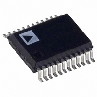
AD7853LARSZ Analog Devices Inc, AD7853LARSZ Datasheet - Page 25

AD7853LARSZ
Manufacturer Part Number
AD7853LARSZ
Description
IC ADC 12BIT SRL 200KSPS 24SSOP
Manufacturer
Analog Devices Inc
Datasheet
1.AD7853LARSZ-REEL.pdf
(34 pages)
Specifications of AD7853LARSZ
Data Interface
8051, QSPI™, Serial, SPI™ µP
Number Of Bits
12
Sampling Rate (per Second)
100k
Number Of Converters
2
Power Dissipation (max)
33mW
Voltage Supply Source
Analog and Digital
Operating Temperature
-40°C ~ 85°C
Mounting Type
Surface Mount
Package / Case
24-SSOP (0.200", 5.30mm Width)
Resolution (bits)
12bit
Sampling Rate
100kSPS
Input Channel Type
Single Ended
Supply Voltage Range - Analog
3V To 5.5V
Supply Voltage Range - Digital
3V To 5.5V
Lead Free Status / RoHS Status
Lead free / RoHS Compliant
REV. B
Mode 2 (3-Wire SPI/QSPI Interface Mode)
This is the DEFAULT INTERFACE MODE.
In Figure 35 below we have the timing diagram for Interface
Mode 2 which is the SPI/QSPI interface mode. Here the SYNC
input is active low and may be pulsed or tied permanently low.
If SYNC is permanently low 16 clock pulses must be applied to
the SCLK pin for the part to operate correctly, and with a
pulsed SYNC input a continuous SCLK may be applied provided
SYNC is low for only 16 SCLK cycles. In Figure 30 the SYNC
going low disables the three-state on the DOUT pin. The first
falling edge of the SCLK after the SYNC going low clocks out
the first leading zero on the DOUT pin. The DOUT pin is
three-stated again a time t
DIN pin the data input has to be set up a time, t
SCLK rising edge as the part samples the input data on the
SCLK rising edge in this case. The POLARITY pin may be
used to change the SCLK edge which the data is sampled on
and clocked out on. If resetting the interface is required, the
SYNC must be taken high and then low.
Mode 3 (QSPI Interface Mode)
Figure 36 shows the timing diagram for Interface Mode 3. In
this mode the DSP is the master and the part is the slave. Here
the SYNC input is edge triggered from high to low, and the 16
clock pulses are counted from this edge. Since the clock pulses
are counted internally then the SYNC signal does not have to go
Figure 35. SPI/QSPI Mode 2 Timing Diagram for Read/Write Operation with DIN Input, DOUT Output and SYNC Input
(SM1 = SM2 = 0)
Figure 36. QSPI Mode 3 Timing Diagram for Read/Write Operation with SYNC Input Edge Triggered (SM1 = 0, SM2 = 1)
DOUT (O/P)
SYNC (I/P)
SCLK (I/P)
DIN (I/P)
DOUT (O/P)
SYNC (I/P)
SCLK (I/P)
DIN (I/P)
POLARITY PIN
LOGIC HIGH
THREE-
STATE
POLAR PIN
LOGIC HIGHITY
t
5
THREE-
STATE
12
t
5
after the SYNC goes high. With the
t
3
DB15
t
t
t
t
7
3
6
11
t
= –0.4 t
= 75/115 MAX (5V/3V), t
1
3
= 20/30 MIN (NONCONTINUOUS SCLK) (5V/3V), (30/50)/0.4 t
DB15
DB15
t
7
t
1
6
t
t
t
3
6
11
DB15
CLKIN
= –0.4 t
= 75/115 MAX (5V/3V), t
DB14
= 20/30 MIN (5V/3V)
t
6
t
8
2
MIN (NONCONTINUOUS SCLK) –/+0.4 t
DB14
DB14
CLKIN
t
8
2
t
9
7
DB14
, before the
DB13
MIN (NONCONTINUOUS SCLK) –/+0.4 t
t
t
3
9
10
7
= 40/60ns MIN (5V/3V), t
DB13
DB13
t
3
10
DB13
DB12
7
= 40/60ns MIN (5V/3V), t
4
t
DB12
DB12
–25–
6
4
t
DB12
6
high after the 16th SCLK rising edge as shown by the dotted
SYNC line in Figure 36. Thus a frame sync that gives a high
pulse, of one SCLK cycle minimum duration, at the beginning
of the read/write operation may be used. The rising edge of
SYNC enables the three-state on the DOUT pin. The falling
edge of SYNC disables the three-state on the DOUT pin, and
data is clocked out on the falling edge of SCLK. Once SYNC
goes high, the three-state on the DOUT pin is enabled. The
data input is sampled on the rising edge of SCLK and thus has
to be valid a time, t
pin may be used to change the SCLK edge which the data is
sampled on and clocked out on. If resetting the interface is
required, the SYNC must be taken high and then low.
Modes 4 and 5 (Self-Clocking Modes)
The timing diagrams in Figure 38 and Figure 39 are for Inter-
face Modes 4 and 5. Interface Mode 4 has a noncontinuous
SCLK output and Interface Mode 5 has a continuous SCLK
output. These modes of operation are especially different to all
the other modes since the SCLK and SYNC are outputs. The
SYNC is generated by the part as is the SCLK. The master
clock at the CLKIN pin is routed directly to the SCLK pin for
Interface Mode 5 (Continuous SCLK) and the CLKIN signal is
gated with the SYNC to give the SCLK (noncontinuous) for
Interface Mode 4.
DB11
5
DB11
DB11
8
= 20/30 MIN (5V/3V),
5
SCLK
DB11
t
DB10
8
MIN/MAX (CONTINUOUS SCLK),
8
6
= 20/30 MIN (5V/3V),
t
DB10
DB10
8
SCLK
SCLK
6
DB10
MIN/MAX (CONTINUOUS SCLK),
= ns MIN/MAX (CONTINUOUS SCLK) (5V/3V)
7
, before this rising edge. The POLARITY
DB0
16
AD7853/AD7853L
DB0
DB0
16
t
11
DB0
t
11
THREE-
STATE
t
THREE-
12
STATE
t
12


