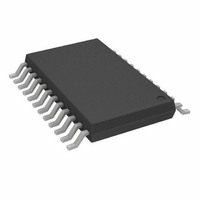
AD7714YRUZ Analog Devices Inc, AD7714YRUZ Datasheet - Page 13

AD7714YRUZ
Manufacturer Part Number
AD7714YRUZ
Description
IC ADC SIGNAL COND 3/5V 24-TSSOP
Manufacturer
Analog Devices Inc
Datasheet
1.AD7714YNZ.pdf
(40 pages)
Specifications of AD7714YRUZ
Data Interface
DSP, MICROWIRE™, QSPI™, Serial, SPI™
Number Of Bits
24
Sampling Rate (per Second)
1k
Number Of Converters
1
Power Dissipation (max)
7mW
Voltage Supply Source
Analog and Digital
Operating Temperature
-40°C ~ 105°C
Mounting Type
Surface Mount
Package / Case
24-TSSOP (0.173", 4.40mm Width)
Resolution (bits)
24bit
Sampling Rate
1kSPS
Input Channel Type
Differential
Supply Voltage Range - Digital
2.7V To 5.25V
Supply Current
1.1mA
Number Of Elements
1
Resolution
24Bit
Architecture
Delta-Sigma
Sample Rate
1KSPS
Input Polarity
Unipolar/Bipolar
Input Type
Voltage
Differential Input
Yes
Power Supply Requirement
Analog and Digital
Single Supply Voltage (typ)
3/5V
Single Supply Voltage (min)
2.7V
Single Supply Voltage (max)
5.25V
Dual Supply Voltage (typ)
Not RequiredV
Dual Supply Voltage (min)
Not RequiredV
Dual Supply Voltage (max)
Not RequiredV
Power Dissipation
4.75mW
Integral Nonlinearity Error
±0.0015%FSR
Operating Temp Range
-40C to 105C
Operating Temperature Classification
Industrial
Mounting
Surface Mount
Pin Count
24
Package Type
TSSOP
Lead Free Status / RoHS Status
Lead free / RoHS Compliant
For Use With
EVAL-AD7714-3EBZ - BOARD EVALUATION FOR AD7714
Lead Free Status / Rohs Status
Compliant
Available stocks
Company
Part Number
Manufacturer
Quantity
Price
Part Number:
AD7714YRUZ
Manufacturer:
ADI/亚德诺
Quantity:
20 000
BUFFERED MODE NOISE
Table III shows the typical output rms noise and effective resolution for some typical notch and –3 dB frequencies for the AD7714-
5 with f
MHz and BUFFER = +5 V. The numbers given are for the bipolar input ranges and are generated with a differential analog input
voltage of 0 V. For the AD7714-5, the V
brackets in each table are for the effective resolution of the part (rounded to the nearest 0.5 LSB). The effective resolution of the
device is defined as the ratio of the output rms noise to the input full scale (i.e., 2 V
calculated using peak-to-peak output noise numbers. Peak-to-peak noise numbers can be up to 6.6 times the rms numbers while
effective resolution numbers based on peak-to-peak noise can be 2.5 bits below the effective resolution based on rms noise as quoted
in the tables.
Filter First
Notch & O/P –3 dB
Data Rate
5 Hz
10 Hz
25 Hz
30 Hz
50 Hz
60 Hz
100 Hz
250 Hz
500 Hz
1 kHz
Filter First
Notch & O/P –3 dB
Data Rate
5 Hz
10 Hz
25 Hz
30 Hz
50 Hz
60 Hz
100 Hz
250 Hz
500 Hz
1 kHz
REV. C
CLK IN
= 2.4576 MHz and BUFFER = +5 V. Table IV gives the information for the AD7714-3 again with f
Frequency
1.31 Hz
2.62 Hz
6.55 Hz
7.86 Hz
13.1 Hz
15.72 Hz
26.2 Hz
65.5 Hz
131 Hz
262 Hz
Frequency
1.31 Hz
2.62 Hz
6.55 Hz
7.86 Hz
13.1 Hz
15.72 Hz
26.2 Hz
65.5 Hz
131 Hz
262 Hz
Table III. AD7714-5 Buffered Mode Output Noise/Resolution for f
Table IV. AD7714-3 Buffered Mode Output Noise/Resolution for f
0.99
1.5
2.5
2.9
4.2
6.1
13.8
87
508
2860 (11)
1.16
1.7
3.5
3.7
4.5
5.3
10
47
300
1722 (10.5) 735
Gain of
Gain of
1
1
(22.5) 0.68 (22)
(21.5) 0.95 (21.5) 0.63 (21)
(21)
(20.5) 1.8
(20)
(19.5) 2.9
(18.5) 6.5
(16)
(13.5) 241
(21)
(20.5) 1
(19.5) 1.8
(19.5) 2.2
(19)
(19)
(18)
(15.5) 29
(13.5) 171
REF
1.7
2.5
56
1700 (10.5) 745 (10.5) 480 (10.5) 197 (10.5) 94
0.76 (20.5) 0.34 (20)
3
3.3
4.9
Gain of
Gain of
voltage is +2.5 V while for the AD7714 the V
2
2
Typical Output RMS Noise in V (Effective Resolution in Bits)
(20.5) 0.88 (20.5) 0.75 (19.5) 0.57 (19)
(20.5) 1
(20)
(19.5) 2
(18.5) 3.5 (18.5) 2.2 (18)
(15.5) 25
(13.5) 117 (13.5) 73
Typical Output RMS Noise in V (Effective Resolution in Bits)
(20.5) 0.7 (20)
(19.5) 1.1 (19)
(19)
(18.5) 1.7 (18.5) 1.0 (18)
(18.5) 1.8 (18.5) 1.1 (18)
(18)
(15.5) 15
(13)
(10.5) 380 (10.5) 230 (10.5) 93
0.46 (21.5) 0.26 (21)
1.5 (19.5) 1.1 (19)
1.3 (19)
3.1 (17.5) 1.5 (17.5) 1.2 (17)
74
Gain of
Gain of
4
4
(20)
(19.5) 1.2 (19)
(15.5) 11
(15.5) 7.5 (15.5) 4.7 (15)
(13)
–13–
0.41 (20.5) 0.39 (19.5) 0.36 (18.5) 0.36 (17.5) 0.36 (16.5)
0.87 (19.5) 0.75 (18.5) 0.72 (17.5) 0.72 (16.5) 0.71 (15.5)
0.29 (20)
0.46 (19.5) 0.45 (18.5) 0.4 (17.5) 0.4 (16.5) 0.4 (15.5)
0.74 (18.5) 0.63 (18)
0.76 (18.5) 0.68 (18)
35
Gain of
Gain of
8
8
(15.5) 5.7 (15.5) 3.6 (15.5) 2.4 (15)
(13)
(13)
0.26 (20)
0.94 (18.5) 0.94 (17.5) 0.94 (16.5) 0.87 (15.5)
1
1.3 (18)
34
0.29 (19)
0.92 (17.5) 0.9 (16.5) 0.89 (15.5) 0.89 (14.5)
1
21
Gain of
Gain of
REF
16
16
/GAIN). It should be noted that it is not
(18.5) 0.97 (17.5) 0.95 (16.5) 0.94 (15.5)
(13)
(17)
(13)
(10.5) 55
REF
CLK IN
CLK IN
voltage is +1.25 V. The numbers in
0.57 (18)
0.96 (16.5) 0.96 (15.5) 0.96 (14.5)
0.26 (19)
1.2 (17)
16
0.28 (18)
0.6 (17)
0.66 (17)
1.2 (16)
2.6 (15)
8.6 (13)
= 2.4576 MHz
= 2.4576 MHz
Gain of
Gain of
32
32
(13)
(10.5) 53
(10.5) 30
0.26 (18)
0.57 (17)
8.5 (13)
0.6 (16)
2.5 (14)
1.3 (16)
0.26 (17)
0.66 (16)
1.2 (15)
5.6 (13)
Gain of
Gain of
64
64
(10.5) 23
(10.5) 12
CLK IN
AD7714
0.26 (17)
0.56 (16)
1.1 (15)
2.1 (14)
5.2 (13)
0.26 (16)
0.6 (15)
1.2 (14)
1.6 (13.5)
3.1 (12.5)
0.66 (15)
Gain of
Gain of
= 2.4576
128
128
(10.5)
(10.5)
2


