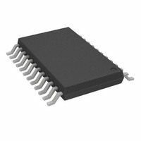
AD7730LBRU Analog Devices Inc, AD7730LBRU Datasheet - Page 12

AD7730LBRU
Manufacturer Part Number
AD7730LBRU
Description
IC ADC TRANSDUCER BRIDGE 24TSSOP
Manufacturer
Analog Devices Inc
Datasheet
1.AD7730LBRUZ.pdf
(52 pages)
Specifications of AD7730LBRU
Rohs Status
RoHS non-compliant
Number Of Bits
24
Sampling Rate (per Second)
600
Data Interface
DSP, Serial, SPI™
Number Of Converters
1
Power Dissipation (max)
125mW
Voltage Supply Source
Analog and Digital
Operating Temperature
-40°C ~ 85°C
Mounting Type
Surface Mount
Package / Case
24-TSSOP (0.173", 4.40mm Width)
For Use With
EVAL-AD7730LEBZ - BOARD EVALUATION FOR AD7730EVAL-AD7730EBZ - BOARD EVAL FOR AD7730
Available stocks
Company
Part Number
Manufacturer
Quantity
Price
Company:
Part Number:
AD7730LBRUZ
Manufacturer:
ADI
Quantity:
1 000
Company:
Part Number:
AD7730LBRUZ-REEL7
Manufacturer:
ADI
Quantity:
1 000
Register Name
Communications
Register
Status Register
Data Register
Mode Register
Filter Register
DAC Register
Offset Register
Gain Register
Test Register
AD7730/AD7730L
WEN ZERO
HIREF
ZERO
ZERO ZERO AC
SF3
MD2
SF11 SF10
RDY
SF2
ZERO
STDY
ZERO
MD1
SF9
SF1
RW1
DAC5
STBY
MD0
RN1
Type
Write Only
Read Only
Read Only
Read/Write
Read/Write
Read/Write
Read/Write
Read/Write
Read/Write
SF8
SF0
CHP
NOREF
RW0
DAC4
RN0
B/U
SF7
ZERO ZERO SKIP
DL3
ZERO
CLKDIS
DAC3
Size
8 Bits
8 Bits
16 Bits or 24 Bits
16 Bits
24 Bits
8 Bits
24 Bits
24 Bits
24 Bits
MS3
DEN
SF6
DL2
Table V. Summary of On-Chip Registers
DAC2
RS2
MS2
D1
BO
SF5
DL1
DAC1
RS1
MS1
CH1
D0
Power-On/Reset
Default Value
Not Applicable
CX Hex
000000 Hex
01B0 Hex
200010 Hex
20 Hex
800000 Hex
59AEE7 Hex
000000 Hex
SF4
FAST
DL0
DAC0
RS0
–12–
MS0
CH0
WL
All operations to other registers are initiated through
Controls functions such as mode of operation, uni-
Controls the amount of averaging in the first stage
Provides control of the amount of correction per-
Contains a 24-bit word which is the offset calibration
Contains a 24-bit word which is the gain calibration
Controls the test modes of the part which are used
Function
the Communications Register. This controls whether
subsequent operations are read or write operations
and also selects the register for that subsequent
operation. Most subsequent operations return con-
trol to the Communications Register except for the
continuous read mode of operation.
Provides status information on conversions, calibra-
tions, settling to step inputs, standby operation and
the validity of the reference voltage.
Provides the most up-to-date conversion result from
the part. Register length can be programmed to be
16 bits or 24 bits.
polar/bipolar operation, controlling the function of
AIN2(+)/D1 and AIN2(-)/D0, burnout current,
Data Register word length and disabling of MCLK
OUT. It also contains the reference selection bit, the
range selection bits and the channel selection bits.
filter, selects the fast step and skip modes and con-
trols the ac excitation and chopping modes on the
part.
formed by the Offset/TARE DAC.
coefficient for the part. The contents of this register
are used to provide offset correction on the output
from the digital filter. There are three Offset Regis-
ters on the part and these are associated with the
input channels as outlined in Table XIII.
coefficient for the part. The contents of this register
are used to provide gain correction on the output
from the digital filter. There are three Gain Registers
on the part and these are associated with the input
channels as outlined in Table XIII.
when testing the part. The user is advised not to
change the contents of this register.
REV. A


