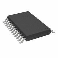
AD7730LBRU Analog Devices Inc, AD7730LBRU Datasheet - Page 36

AD7730LBRU
Manufacturer Part Number
AD7730LBRU
Description
IC ADC TRANSDUCER BRIDGE 24TSSOP
Manufacturer
Analog Devices Inc
Datasheet
1.AD7730LBRUZ.pdf
(52 pages)
Specifications of AD7730LBRU
Rohs Status
RoHS non-compliant
Number Of Bits
24
Sampling Rate (per Second)
600
Data Interface
DSP, Serial, SPI™
Number Of Converters
1
Power Dissipation (max)
125mW
Voltage Supply Source
Analog and Digital
Operating Temperature
-40°C ~ 85°C
Mounting Type
Surface Mount
Package / Case
24-TSSOP (0.173", 4.40mm Width)
For Use With
EVAL-AD7730LEBZ - BOARD EVALUATION FOR AD7730EVAL-AD7730EBZ - BOARD EVAL FOR AD7730
Available stocks
Company
Part Number
Manufacturer
Quantity
Price
Company:
Part Number:
AD7730LBRUZ
Manufacturer:
ADI
Quantity:
1 000
Company:
Part Number:
AD7730LBRUZ-REEL7
Manufacturer:
ADI
Quantity:
1 000
AD7730/AD7730L
In DSP applications, the SCLK is generally a continuous clock.
In these applications, the CS input for the AD7730 is generated
from a frame synchronization signal from the DSP. In these
applications, the first edge after CS goes low is the active edge.
The MSB of the data to be shifted into the DSP must be set up
prior to this first active edge. Unlike microcontroller applica-
tions, the DSP does not provide a clock edge to clock the MSB
from the AD7730. In this case, the CS of the AD7730 places
the MSB on the DOUT line. For processors with the rising edge
of SCLK as the active edge, the POL input should be tied high.
In this case, the DSP takes data on the rising edge. If CS goes
low while SCLK is low, the MSB is clocked out on the DOUT
line from the CS. Subsequent data bits are clocked from the
falling edge of SCLK. For processors with the falling edge of
SCLK as the active edge, the POL input should be tied low. In
this case, the DSP takes data on the falling edge. If CS goes low
while SCLK is high, the MSB is clocked out on the DOUT line
from the CS. Subsequent data bits are clocked from the rising
edge of SCLK.
(POL = 1)
(POL = 0)
(POL = 1)
(POL = 0)
DOUT
SCLK
SCLK
SCLK
SCLK
RDY
CS
DIN
CS
t
5A
t
12
t
t
4
11
t
3
Figure 19. Write Cycle Timing Diagram
Figure 18. Read Cycle Timing Diagram
MSB
t
MSB
5
t
13
t
t
6
14
t
t
7
15
–36–
The RDY line is used as a status signal to indicate when data is
ready to be read from the AD7730’s data register. RDY goes
low when a new data word is available in the data register. It is
reset high when a read operation from the data register is com-
plete. It also goes high prior to the updating of the data register
to indicate when a read from the data register should not be
initiated. This is to ensure that the transfer of data from the data
register to the output shift register does not occur while the data
register is being updated. It is possible to read the same data
twice from the output register even though the RDY line returns
high after the first read operation. Care must be taken, however,
to ensure that the read operations are not initiated as the next
output update is about to take place.
For systems with a single data line, the DIN and DOUT lines
on the AD7730 can be connected together, but care must be
taken in this case not to place the part in continuous read mode
as the part monitors DIN while supplying data on DOUT and
as a result, it may not be possible to take the part out of its
continuous read mode.
t
t
6
14
t
t
7
15
LSB
LSB
t
10
t
9
t
t
8
16
REV. A


