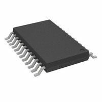
AD7730LBRU Analog Devices Inc, AD7730LBRU Datasheet - Page 15

AD7730LBRU
Manufacturer Part Number
AD7730LBRU
Description
IC ADC TRANSDUCER BRIDGE 24TSSOP
Manufacturer
Analog Devices Inc
Datasheet
1.AD7730LBRUZ.pdf
(52 pages)
Specifications of AD7730LBRU
Rohs Status
RoHS non-compliant
Number Of Bits
24
Sampling Rate (per Second)
600
Data Interface
DSP, Serial, SPI™
Number Of Converters
1
Power Dissipation (max)
125mW
Voltage Supply Source
Analog and Digital
Operating Temperature
-40°C ~ 85°C
Mounting Type
Surface Mount
Package / Case
24-TSSOP (0.173", 4.40mm Width)
For Use With
EVAL-AD7730LEBZ - BOARD EVALUATION FOR AD7730EVAL-AD7730EBZ - BOARD EVAL FOR AD7730
Available stocks
Company
Part Number
Manufacturer
Quantity
Price
Company:
Part Number:
AD7730LBRUZ
Manufacturer:
ADI
Quantity:
1 000
Company:
Part Number:
AD7730LBRUZ-REEL7
Manufacturer:
ADI
Quantity:
1 000
REV. A
Data Register (RS2–RS0 = 0, 0, 1); Power On/Reset Status: 000000 Hex
The Data Register on the part is a read-only register which contains the most up-to-date conversion result from the AD7730. Fig-
ure 5 shows a flowchart for reading from the registers on the AD7730. The register can be programmed to be either 16 bits or 24 bits
wide, determined by the status of the WL bit of the Mode Register. The RDY output and RDY bit of the Status Register are set low
when the Data Register is updated. The RDY pin and RDY bit will return high once the full contents of the register (either 16 bits or
24 bits) have been read. If the Data Register has not been read by the time the next output update occurs, the RDY pin and RDY bit
will go high for at least 100
the Data Register as it is being updated. Once the updating of the Data Register has taken place, RDY returns low.
If the Communications Register data sets up the part for a write operation to this register, a write operation must actually take place
in order to return the part to where it is expecting a write operation to the Communications Register (the default state of the inter-
face). However, the 16 or 24 bits of data written to the part will be ignored by the AD7730.
Mode Register (RS2–RS0 = 0, 1, 0); Power On/Reset Status: 01B0 Hex
The Mode Register is a 16-bit register from which data can be read or to which data can be written. This register configures
the operating modes of the AD7730, the input range selection, the channel selection and the word length of the Data Register.
Table X outlines the bit designations for the Mode Register. MR0 through MR15 indicate the bit location, MR denoting the bits are
in the Mode Register. MR15 denotes the first bit of the data stream. The number in brackets indicates the power-on/reset default
status of that bit. Figure 5 shows a flowchart for reading from the registers on the AD7730 and Figure 6 shows a flowchart for writ-
ing to the registers on the part.
Bit
Location
MR15–MR13
HIREF (1)
MD2 (0)
MR15
MR7
Bit
Mnemonic
MD2–MD0
ZERO (0)
MD1 (0)
MR14
MR6
t
CLK IN
, indicating when a read from the Data Register should not be initiated to avoid a transfer from
Description
Mode Bits. These three bits determine the mode of operation of the AD7730 as outlined in
Table XI. The modes are independent, such that writing new mode bits to the Mode Register
will exit the part from the mode in which it is operating and place it in the new requested mode
immediately after the Mode Register write. The function of the mode bits is described in more
detail below.
MD2
0
0
0
0
1
1
1
1
MD0 (0)
RN1 (1)
MR13
MR5
MD1
0
0
1
1
0
0
1
1
Table XI. Operating Modes
Table X. Mode Register
RN0 (1)
B/U (0)
MR12
MR4
MD0
0
1
0
1
0
1
0
1
–15–
CLKDIS (0)
DEN (0)
Mode of Operation
Sync (Idle) Mode
Continuous Conversion Mode
Single Conversion Mode
Power-Down (Standby) Mode
Internal Zero-Scale Calibration
Internal Full-Scale Calibration
System Zero-Scale Calibration
System Full-Scale Calibration
MR11
MR3
D1 (0)
BO (0)
MR10
MR2
Power-On/Reset Default
CH1 (0)
D0 (0)
MR9
MR1
AD7730/AD7730L
CH0 (0)
WL (1)
MR8
MR0


