ADC1207S080HW/C1,5 NXP Semiconductors, ADC1207S080HW/C1,5 Datasheet
ADC1207S080HW/C1,5
Specifications of ADC1207S080HW/C1,5
Available stocks


Related parts for ADC1207S080HW/C1,5


ADC1207S080HW/C1,5 Summary of contents
Page 1
ADC1207S080 Single 12 bits ADC MHz with direct/ultra high IF sampling Rev. 02 — 7 August 2008 1. General description The ADC1207S080 is a 12-bit Analog-to-Digital Converter (ADC) optimized for direct Input Frequency (IF) sampling and supporting ...
Page 2
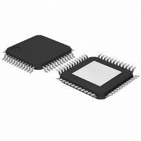
... NXP Semiconductors 3. Applications High speed analog to digital conversion for: I Radio transceivers I Wireless infrastructure I Cable modem I Digital storage scope I Fixed telecommunication, I Optical networking I Wireless Local Area Network (WLAN) infrastructure. I General purpose applications 4. Ordering information Table 1. Ordering information Type number Package Name ADC1207S080HW HTQFP48 5 ...
Page 3
... NXP Semiconductors 6. Pinning information 6.1 Pinning Fig 2. Pin configuration 6.2 Pin description Table 2. Symbol n.c. AGND1 IN CMADC INN AGND1 DEC n.c. FSOUT FSIN n.c. n.c. n.c. DEL1 DEL0 V CCD2 ADC1207S080_2 Product data sheet Single 12 bits ADC MHz with direct/ultra high IF sampling n ...
Page 4
... NXP Semiconductors Table 2. Symbol DGND2 CE_N OTC OGND V CCO OGND V CCO IR D11 D10 CCS DGND1 CLKN CLK V CCD1 DGND1 AGND2 V CCA2 V CCA1 AGND1 V CCA1 AGND1 DGND [1] P: power supply; G: ground; I: input; O: output. ADC1207S080_2 Product data sheet Single 12 bits ADC MHz with direct/ultra high IF sampling Pin description … ...
Page 5
... NXP Semiconductors 7. Limiting values Table 3. In accordance with the Absolute Maximum Rating System (IEC 60134). Symbol V CCA V CCD V CCO i(IN) V i(INN) V i(CLK) V i(CLKN stg T amb T j [1] The supply voltages V supply voltage differences V [2] The supply voltage V differences V 8. Thermal characteristics Table 4. ...
Page 6
... NXP Semiconductors 9. Characteristics Table 5. Characteristics CCA CCD to + 0.5 dBFS; V i(IN) i(INN 3 CCA CCD CCO Symbol Parameter Supplies V analog supply voltage CCA V digital supply voltage CCD V output supply voltage CCO I analog supply current CCA I digital supply current CCD I output supply current ...
Page 7
... NXP Semiconductors Table 5. Characteristics …continued CCA CCD to + 0.5 dBFS; V i(IN) i(INN 3 CCA CCD CCO Symbol Parameter I LOW-level input current IL I HIGH-level input current V IH Digital inputs: pins DEL0 and DEL1 V LOW-level input voltage IL V HIGH-level input voltage IH I LOW-level input current ...
Page 8
... NXP Semiconductors Table 5. Characteristics …continued CCA CCD to + 0.5 dBFS; V i(IN) i(INN 3 CCA CCD CCO Symbol Parameter Clock timing inputs: pins CLK and CLKN duty cycle f minimum clock clk(min) frequency f maximum clock clk(max) frequency Timing complete conversion signal: pin CCS; see ...
Page 9
... NXP Semiconductors Table 5. Characteristics …continued CCA CCD to + 0.5 dBFS; V i(IN) i(INN 3 CCA CCD CCO Symbol Parameter S/N signal-to-noise ratio SFDR spurious free dynamic range ACPR adjacent channel power ratio IMD2 second-order intermodulation distortion IMD3 third-order intermodulation distortion [1] The circuit has two clock inputs: CLK and CLKN. There are 5 modes of operation: ...
Page 10
... NXP Semiconductors 10. Additional information relating to Table i(IN) Code Underfl 2047 4094 4095 Overflow Table 7. Two’s complement output (OTC) Chip enable input (CE_N) Data output (D0 to D11; IR [ don’t care. Fig 3. Output timing diagram ADC1207S080_2 Product data sheet ...
Page 11
... NXP Semiconductors power spectrum (dBc) (1) f (2) f (3) f (4) f (5) f (6) f Fig 4. V i(a)(p-p) (V) Fig 5. The ADC1207S080 allows modifying the ADC full-scale. This could be done with FSIN (full-scale input) according to ADC1207S080_2 Product data sheet Single 12 bits ADC MHz with direct/ultra high IF sampling ...
Page 12
... NXP Semiconductors The ADC1207S080 generates an adjustable clock output called Complete Conversion Signal (CCS), which can be used to control the acquisition of converted output data by the digital circuit connected to the ADC1207S080 output data bus. Two logic inputs, DEL0 and DEL1 pins, allow adjusting the delay of the edge of the CCS signal to achieve an optimal position in the stable, usable zone of the data ...
Page 13
... NXP Semiconductors 11. Definitions 11.1 Static parameters 11.1.1 Integral Non-Linearity (INL defined as the deviation of the transfer function from a best fit straight line (linear regression computation). The INL of the code i is obtained from the equation: INL i where: S corresponds to the slope of the ideal straight line (code width); i corresponds to the code value ...
Page 14
... NXP Semiconductors Remark: In the following equations, P effects of random noise, non-linearities, sampling time errors, and ‘quantization noise’. 11.2.1 SIgnal-to-Noise And Distortion (SINAD) The ratio of the output signal power to the noise plus distortion power for a given sample rate and input frequency, excluding the DC component: SINAD dB 11 ...
Page 15
... NXP Semiconductors 11.2.6 IMD2 (IMD3) magnitude Fig 8. Spectral of dual tone input sine wave with frequency From a dual tone input sinusoid (f the coherence criterion), the intermodulation distortion products IMD2 and IMD3 (respectively, 2nd and 3rd order components) are defined, as follows. The ratio of the RMS value of either tone to the RMS value of the worst second (third) order intermodulation product ...
Page 16
... NXP Semiconductors 12. Application information 12.1 ADC1207S080 in 3G radio receivers The ADC1207S080 has been proven in many 3G radio receivers with various operating conditions regarding Input Frequency (IF), signal IF bandwidth and sampling frequency. The ADC1207S080 is provided with a maximum analog input signal frequency of 400 MHz. It allows a significant cost-down of the RF front-end, from two mixers to only one, even in multi-carriers architecture ...
Page 17
... NXP Semiconductors 12.2 Application diagram 330 nF ADT1_1WT 3 6 100 5 2 n.c. IN 100 100 10 nF analog ground digital ground GND XX Fig 10. Application diagram ADC1207S080_2 Product data sheet Single 12 bits ADC MHz with direct/ultra high IF sampling V CCA n.c. 1 AGND1 CMADC 4 INN 5 AGND1 6 ADC1207S080 ...
Page 18
... NXP Semiconductors 13. Package outline HTQFP48: plastic thermal enhanced thin quad flat package; 48 leads; body mm; exposed die pad y exposed die pad side pin 1 index DIMENSIONS (mm are the original dimensions) A UNIT max. 0.15 1.05 0.27 1.2 mm 0.25 0.05 0.95 0.17 Note 1. Plastic or metal protrusions of 0.25 mm maximum per side are not included. ...
Page 19
... NXP Semiconductors 14. Revision history Table 10. Revision history Document ID Release date ADC1207S080_2 20080807 • Modifications: Corrections made to version number in • Corrections made to several entries in • Corrections made to alignment in • Corrections made to ADC1207S080_1 20080611 ADC1207S080_2 Product data sheet Single 12 bits ADC MHz with direct/ultra high IF sampling ...
Page 20
... Right to make changes — NXP Semiconductors reserves the right to make changes to information published in this document, including without limitation specifications and product descriptions, at any time and without notice ...
Page 21
... NXP Semiconductors 17. Contents 1 General description . . . . . . . . . . . . . . . . . . . . . . 1 2 Features . . . . . . . . . . . . . . . . . . . . . . . . . . . . . . . 1 3 Applications . . . . . . . . . . . . . . . . . . . . . . . . . . . . 2 4 Ordering information . . . . . . . . . . . . . . . . . . . . . 2 5 Block diagram . . . . . . . . . . . . . . . . . . . . . . . . . . 2 6 Pinning information . . . . . . . . . . . . . . . . . . . . . . 3 6.1 Pinning . . . . . . . . . . . . . . . . . . . . . . . . . . . . . . . 3 6.2 Pin description . . . . . . . . . . . . . . . . . . . . . . . . . 3 7 Limiting values Thermal characteristics Characteristics . . . . . . . . . . . . . . . . . . . . . . . . . . 6 10 Additional information relating to 11 Definitions . . . . . . . . . . . . . . . . . . . . . . . . . . . . 13 11.1 Static parameters . . . . . . . . . . . . . . . . . . . . . . 13 11.1.1 Integral Non-Linearity (INL ...