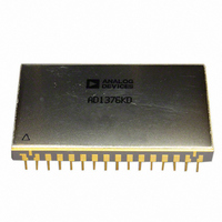
ADADC80-12 Analog Devices Inc, ADADC80-12 Datasheet - Page 11

ADADC80-12
Manufacturer Part Number
ADADC80-12
Description
IC ADC 12-BIT INTEGRATED 32-CDIP
Manufacturer
Analog Devices Inc
Datasheet
1.ADADC80-12.pdf
(16 pages)
Specifications of ADADC80-12
Data Interface
Parallel
Rohs Status
RoHS non-compliant
Number Of Bits
12
Sampling Rate (per Second)
40k
Number Of Converters
1
Power Dissipation (max)
800mW
Voltage Supply Source
Analog and Digital, Dual ±
Operating Temperature
-25°C ~ 85°C
Mounting Type
Through Hole
Package / Case
32-CDIP (0.900", 22.86mm)
Resolution (bits)
12bit
Input Channel Type
Single Ended
Supply Current
70mA
Digital Ic Case Style
DIP
No. Of Pins
32
Operating Temperature Range
-25°C To +85°C
Number Of Elements
1
Resolution
12Bit
Architecture
SAR
Input Polarity
Unipolar/Bipolar
Input Type
Voltage
Rated Input Volt
5/10/±2.5/±5/±10V
Differential Input
No
Power Supply Requirement
Dual
Single Supply Voltage (typ)
Not RequiredV
Single Supply Voltage (min)
Not RequiredV
Single Supply Voltage (max)
Not RequiredV
Dual Supply Voltage (typ)
±15/5V
Dual Supply Voltage (min)
±14/4.75V
Dual Supply Voltage (max)
±16/5.25V
Differential Linearity Error
±0.5LSB(Typ)
Integral Nonlinearity Error
±0.012%FSR
Operating Temp Range
-25C to 85C
Operating Temperature Classification
Commercial
Mounting
Through Hole
Pin Count
32
Package Type
SBCDIP
Input Signal Type
Single-Ended
Lead Free Status / Rohs Status
Not Compliant
Available stocks
Company
Part Number
Manufacturer
Quantity
Price
Part Number:
ADADC80-12
Manufacturer:
AD
Quantity:
20 000
CALIBRATION
External zero adjustment and gain adjustment potentiometers,
connected as shown in Figure 13 and Figure 14, are used for
device calibration. To prevent interaction of these two adjustments,
zero is always adjusted first and gain second. Zero is adjusted
with the analog input near the most negative end of the analog
range (0 for unipolar and −FS for bipolar input ranges). Gain is
adjusted with the analog input near the most positive end of the
analog range.
0 V to 10 V Range
Set analog input to +1 LSB = 0.0024 V; adjust zero for digital
output = 111111111110. Zero is now calibrated. Set analog
+15V
+15V
–15V
–15V
+
+
+
+
24
17
15
25
24
17
15
25
REF OUT
(6.3V)
15V OR 12V
ANALOG
GND
–15V OR
–12V
REF OUT
(6.3V)
15V OR 12V
ANALOG
GND
–15V OR
–12V
+5V
Figure 13. Analog and Power Connections for Unipolar 0 V to 10 V Input Range
+5V
Figure 14. Analog and Power Connections for Bipolar ±10 V Input Range
10kΩ
10kΩ
–15V
+15V
–15V
+15V
5V DIGITAL
5V DIGITAL
SUPPLY
SUPPLY
ADADC80
ADADC80
9
9
+
+
REF
REF
10MΩ
10MΩ
DIGITAL
DIGITAL
10
10
GND
GND
ADJUST
ADJUST
0.01µF
0.01µF
GAIN
GAIN
Rev. E | Page 11 of 16
16
16
BIPOLAR
BIPOLAR
OFFSET
OFFSET
OUT
OUT
12
12
input to +FSR − 2 LSB = 9.9952 V; adjust gain for 000000000001
digital output code. Full-scale gain is now calibrated. For half-
scale calibration check, set analog input to 5.0000 V; digital
output code should be 011111111111.
−10 V to +10 V Range
Set analog input to −9.9951 V; adjust zero for 111111111110
digital output (complementary offset binary) code. Set analog
input to +9.9902 V; adjust gain for 000000000001 digital output
(complementary offset binary) code. For half-scale calibration
check, set analog input to 0.0000 V; digital output (complemen-
tary offset binary) code should be 011111111111.
SPAN
SPAN
ANALOG
20V
20V
INPUT
IN
IN
14
14
DAC
DAC
SAR
SPAN
SAR
SPAN
10V
10V
ANALOG
IN
IN
INPUT
13
13
COMPARATOR
COMPARATOR
IN
IN
11
11
1.8MΩ
1.8MΩ
COMPARATOR
COMPARATOR
+15V
+15V
–15V
–15V
10kΩ
10kΩ
ADADC80


