ADADC80-12 Analog Devices Inc, ADADC80-12 Datasheet - Page 6
ADADC80-12
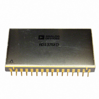
Manufacturer Part Number
ADADC80-12
Description
IC ADC 12-BIT INTEGRATED 32-CDIP
Manufacturer
Analog Devices Inc
Datasheet
1.ADADC80-12.pdf
(16 pages)
Specifications of ADADC80-12
Data Interface
Parallel
Rohs Status
RoHS non-compliant
Number Of Bits
12
Sampling Rate (per Second)
40k
Number Of Converters
1
Power Dissipation (max)
800mW
Voltage Supply Source
Analog and Digital, Dual ±
Operating Temperature
-25°C ~ 85°C
Mounting Type
Through Hole
Package / Case
32-CDIP (0.900", 22.86mm)
Resolution (bits)
12bit
Input Channel Type
Single Ended
Supply Current
70mA
Digital Ic Case Style
DIP
No. Of Pins
32
Operating Temperature Range
-25°C To +85°C
Number Of Elements
1
Resolution
12Bit
Architecture
SAR
Input Polarity
Unipolar/Bipolar
Input Type
Voltage
Rated Input Volt
5/10/±2.5/±5/±10V
Differential Input
No
Power Supply Requirement
Dual
Single Supply Voltage (typ)
Not RequiredV
Single Supply Voltage (min)
Not RequiredV
Single Supply Voltage (max)
Not RequiredV
Dual Supply Voltage (typ)
±15/5V
Dual Supply Voltage (min)
±14/4.75V
Dual Supply Voltage (max)
±16/5.25V
Differential Linearity Error
±0.5LSB(Typ)
Integral Nonlinearity Error
±0.012%FSR
Operating Temp Range
-25C to 85C
Operating Temperature Classification
Commercial
Mounting
Through Hole
Pin Count
32
Package Type
SBCDIP
Input Signal Type
Single-Ended
Lead Free Status / Rohs Status
Not Compliant
Available stocks
Company
Part Number
Manufacturer
Quantity
Price

Part Number:
ADADC80-12
Manufacturer:
AD
Quantity:
20 000


ADADC80
PIN CONFIGURATION AND FUNCTION DESCRIPTIONS
Table 3. Pin Function Descriptions
Pin No.
1 to 6
7
8
9
10
11
12
13
14
15
16
17
18
19
20
21
22
23
24
25
26
27 to 32
Mnemonic
NC
BIT 1 (MSB)
5V DIGITAL SUPPLY
DIGITAL GND
COMPARATOR IN
BIPOLAR OFFSET OUT
10V SPAN IN
20V SPAN IN
ANALOG GND
GAIN ADJUST
15V OR 12V
CONVERT START
EXTERNAL CLOCK IN
CLOCK INHIBIT
SHORT CYCLE
STATUS
CLOCK OUT
REF OUT (6.3V)
−15V OR −12V
NC
BIT 6 to BIT 1 (MSB)
BIT 12 (LSB) to BIT 7
BIPOLAR OFFSET OUT
5V DIGITAL SUPPLY
COMPARATOR IN
Function
Digital Outputs.
No Connection.
MSB Inverted Digital Output.
Digital Positive Supply (Nominally ±0.25 V).
Digital Ground.
Offset Adjust.
Bipolar Offset Output.
Analog Input 10 V Signal Range.
Analog Input 20 V Signal Range.
Analog Ground.
Gain Adjust.
Analog Positive Supply (Nominally ±1.0 V for +15 V or ±0.6 V for +12 V).
Enables Conversion.
External Clock Input.
Clock Inhibit.
Shortens Conversion Cycle to Desired Resolution.
Logic High, ADC Converting/Logic Low, ADC Data Valid.
Internal Clock Output.
6.3 V Reference Output.
Analog Negative Supply (Nominally ±1.0 V for −15 V or ±0.6 V for −12 V).
No Connection.
Digital Outputs.
ANALOG GND
GAIN ADJUST
DIGITAL GND
10V SPAN IN
20V SPAN IN
BIT 1 (MSB)
BIT 1 (MSB)
BIT 6
BIT 5
BIT 4
BIT 3
BIT 2
NC
Figure 2. Pin Configuration
10
12
13
14
15
16
11
1
2
3
4
5
6
7
8
9
Rev. E | Page 6 of 16
NC = NO CONNECT
(Not to Scale)
ADADC80
TOP VIEW
32
31
30
29
28
27
26
25
24
23
22
21
20
19
18
17
BIT 7
BIT 8
BIT 9
BIT 10
BIT 11
BIT 12 (LSB)
NC
–15V OR –12V
REF OUT (6.3V)
CLOCK OUT
STATUS
SHORT CYCLE
CLOCK INHIBIT
EXTERNAL CLOCK IN
CONVERT START
15V OR 12V
Related parts for ADADC80-12
Image
Part Number
Description
Manufacturer
Datasheet
Request
R

Part Number:
Description:
IC ADC 12BIT INTEGRATED 32-CDIP
Manufacturer:
Analog Devices Inc
Datasheet:

Part Number:
Description:
±1.7g Dual-Axis IMEMS Accelerometer Evaluation Board
Manufacturer:
Analog Devices Inc
Datasheet:

Part Number:
Description:
Inertial Sensor Evaluation System
Manufacturer:
Analog Devices Inc
Datasheet:
Part Number:
Description:
Manufacturer:
Analog Devices Inc
Datasheet:
Part Number:
Description:
Manufacturer:
Analog Devices Inc
Datasheet:
Part Number:
Description:
Manufacturer:
Analog Devices Inc
Datasheet:
Part Number:
Description:
Manufacturer:
Analog Devices Inc
Datasheet:
Part Number:
Description:
Manufacturer:
Analog Devices Inc
Datasheet:
Part Number:
Description:
Manufacturer:
Analog Devices Inc
Datasheet:
Part Number:
Description:
Manufacturer:
Analog Devices Inc
Datasheet:
Part Number:
Description:
Manufacturer:
Analog Devices Inc
Datasheet:
Part Number:
Description:
Manufacturer:
Analog Devices Inc
Datasheet:
Part Number:
Description:
Manufacturer:
Analog Devices Inc
Datasheet: