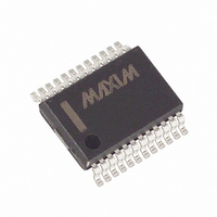
MAX113CAG+T Maxim Integrated Products, MAX113CAG+T Datasheet - Page 10

MAX113CAG+T
Manufacturer Part Number
MAX113CAG+T
Description
IC ADC 8BIT 400KSPS 24-SSOP
Manufacturer
Maxim Integrated Products
Datasheet
1.MAX113CAG.pdf
(12 pages)
Specifications of MAX113CAG+T
Number Of Bits
8
Sampling Rate (per Second)
400k
Data Interface
Parallel
Number Of Converters
3
Power Dissipation (max)
640mW
Voltage Supply Source
Single Supply
Operating Temperature
0°C ~ 70°C
Mounting Type
Surface Mount
Package / Case
24-SSOP
Lead Free Status / RoHS Status
Lead free / RoHS Compliant
When power is first applied, perform a conversion to
initialize the MAX113/MAX117. Disregard the output
data.
Use a 4.7µF electrolytic in parallel with a 0.1µF ceramic
capacitor to bypass V
lead lengths.
Bypass the reference inputs with 0.1µF capacitors, as
shown in Figures 7a, 7b, and 7c.
Figure 8 shows the equivalent circuit of the MAX113/
MAX117 input. When a conversion starts and WR is
low, V
During this acquisition phase, the input capacitors
charge to the input voltage through the resistance of
the internal analog switches. In addition, about 22pF of
stray capacitance must be charged. The input can be
modeled as an equivalent RC network (Figure 9). As
source impedance increases, the capacitors take
longer to charge.
The typical 32pF input capacitance allows source resis-
tance as high as 1.5kΩ without setup problems. For
larger resistances, the acquisition time (t
increased.
Internal protection diodes, which clamp the analog
input to V
swing from GND - 0.3V to V
However, for accurate conversions near full scale and
zero scale the inputs must not exceed V
than 50mV or be lower than GND by 50mV.
+3V, 400ksps, 4/8-Channel,
8-Bit ADCs with 1µA Power-Down
Figure 7d. An N-channel MOSFET switches off the reference
load during power-down
10
* IRML2402
______________________________________________________________________________________
PWRDN
IN_
+3V
DD
is connected to sixteen 0.6pF capacitors.
and GND, allow the channel input pins to
MAX872
N-FET*
DD
0.1µF
to GND. Minimize capacitor
C1
4.7µF
DD
+ 0.3V without damage.
0.1µF
Initial Power-Up
V
REF+
REF-
PWRDN
DD
Analog Inputs
MAX113
MAX117
ACQ
Bypassing
DD
) must be
by more
Figure 8. Equivalent Input Circuit
Figure 9. RC Network Equivalent Input Model
Figure 10. Transfer Function
V
V
00000011
00000010
00000001
00000000
REF-
IN2
11111111
11111110
11111101
OUTPUT CODE
R
V
IN
IN_
1
R
.
.
.
MUX
1
2
V
IN
3
INPUT VOLTAGE (LSBs)
22pF
2k
R
MAX113
MAX117
ON
FULL-SCALE
TRANSITION
T/H
10pF
MAX113
MAX117
1LSB =
FS - 1LSB
V
REF+
256
FS
- V
REF-
V
REF+


