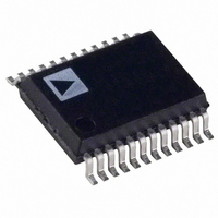
AD7853ARS Analog Devices Inc, AD7853ARS Datasheet - Page 16

AD7853ARS
Manufacturer Part Number
AD7853ARS
Description
IC ADC 12BIT SRL 200KSPS 24-SSOP
Manufacturer
Analog Devices Inc
Datasheet
1.AD7853LARSZ-REEL.pdf
(34 pages)
Specifications of AD7853ARS
Rohs Status
RoHS non-compliant
Number Of Bits
12
Sampling Rate (per Second)
200k
Data Interface
8051, QSPI™, Serial, SPI™ µP
Number Of Converters
2
Power Dissipation (max)
33mW
Voltage Supply Source
Analog and Digital
Operating Temperature
-40°C ~ 85°C
Mounting Type
Surface Mount
Package / Case
24-SSOP (0.200", 5.30mm Width)
AD7853/AD7853L
Input Ranges
The analog input range for the AD7853/AD7853L is 0 V to
V
The only difference between the unipolar range and the bipolar
range is that in the bipolar range the AIN(–) has to be biased up
to +V
Table V and Figures 14 and 15). The unipolar or bipolar mode
is selected by the AMODE pin (0 for the unipolar range and 1
for the bipolar range).
Analog Input
Range
0 V to V
NOTES
1
2
Note that the AIN(–) pin on the AD7853/AD7853L can be
biased up above AGND in the unipolar mode also, if required.
The advantage of biasing the lower end of the analog input
range away from AGND is that the user does not have to have
the analog input swing all the way down to AGND. This has the
advantage in true single supply applications that the input am-
plifier does not have to swing all the way down to AGND. The
upper end of the analog input range is shifted up by the same
amount. Care must be taken so that the bias applied does not
shift the upper end of the analog input above the AV
In the case where the reference is the supply, AV
must be tied to AGND in unipolar mode.
Transfer Functions
For the unipolar range the designed code transitions occur
midway between successive integer LSB values (i.e., 1/2 LSB,
3/2 LSBs, 5/2 LSBs . . . FS –3/2 LSBs). The output coding is
straight binary for the unipolar range with 1 LSB = FS/4096 =
3.3 V/4096 = 0.8 mV when V
transfer characteristic for the unipolar range is shown in
Figure 16.
Output code format is straight binary.
Range is V
UNIPOLAR ANALOG
V
REF
–V
REF
REF
V
INPUT RANGE
Figure 14. 0 to V
in both the unipolar and bipolar ranges.
REF
IN
/2
/2 TO +V
= 0 TO V
SELECTED
2
+3V TO +5V
REF
/2 and the output coding is twos complement (See
REF
1
V
/2 biased about V
REF
REF
Figure 13. Analog Input Buffering
Table V. Analog Input Connections
REF
V
/2
IN
/2
Input Connections Connection
AIN(+)
V
V
IN
IN
10k
10k
10k
REF
AIN(+)
AIN(–)
AMODE
REF
IC1
Unipolar Input Configuration
AIN(–)
AGND
V
V+
V–
/2. Output code format is twos complement.
REF
10k
REF
AD820
AD820-3V
= 3.3 V. The ideal input/output
/2
10 F
AD7853/AD7853L
TRACK AND HOLD
50
AMPLIFIER
Diagram
Figure 14
Figure 15
10nF
(NPO)
0.1 F
DD
TO AIN(+) OF
AD7853/AD7853L
DOUT
, the AIN(–)
DD
AMODE
DGND
DV
STRAIGHT
BINARY
FORMAT
supply.
DD
–16–
Figure 15 shows the AD7853/AD7853L’s V
log input configuration (where AIN(+) cannot go below 0 V so
for the full bipolar range then the AIN(–) pin should be biased
to +V
midway between successive integer LSB values. The output
coding is twos complement with 1 LSB = 4096 = 3.3 V/4096 =
0.8 mV. The ideal input/output transfer characteristic is shown
in Figure 17.
V
Figure 15. V
INPUT RANGE
IN
= 0 TO V
SELECTED
BIPOLAR
Figure 16. Unipolar Transfer Characteristic
ANALOG
REF
V
REF
/2). Once again the designed code transitions occur
111...111
111...110
111...101
111...100
000...011
000...010
000...001
000...000
OUTPUT
011...111
011...110
000...001
000...000
111...111
100...010
100...001
100...000
REF
OUTPUT
Figure 17. Bipolar Transfer Characteristic
DV
/2
CODE
CODE
DD
REF
0V
/2 about V
1LSB
0V
AIN(+)
AMODE
AIN(–)
V
V
IN
IN
= (AIN(+) – AIN(–)), INPUT VOLTAGE
= (AIN(+) – AIN(–)), INPUT VOLTAGE
(V
REF
REF
AD7853/AD7853L
TRACK AND HOLD
/2) –1 LSB
/2 Bipolar Input Configuration
AMPLIFIER
(V
V
REF
REF
/2
/2) +1 LSB
1LSB =
1LSB =
FS = V
4096
REF
+FS –1LSB
FS
4096
+ FS
REF
FS
DOUT
V
/2 bipolar ana-
– 1 LSB
2S
COMPLEMENT
FORMAT
REV. B


