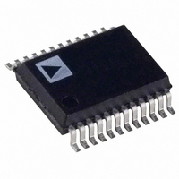
AD7853ARS Analog Devices Inc, AD7853ARS Datasheet - Page 3

AD7853ARS
Manufacturer Part Number
AD7853ARS
Description
IC ADC 12BIT SRL 200KSPS 24-SSOP
Manufacturer
Analog Devices Inc
Datasheet
1.AD7853LARSZ-REEL.pdf
(34 pages)
Specifications of AD7853ARS
Rohs Status
RoHS non-compliant
Number Of Bits
12
Sampling Rate (per Second)
200k
Data Interface
8051, QSPI™, Serial, SPI™ µP
Number Of Converters
2
Power Dissipation (max)
33mW
Voltage Supply Source
Analog and Digital
Operating Temperature
-40°C ~ 85°C
Mounting Type
Surface Mount
Package / Case
24-SSOP (0.200", 5.30mm Width)
Parameter
LOGIC OUTPUTS
CONVERSION RATE
POWER REQUIREMENTS
SYSTEM CALIBRATION
NOTES
1
2
3
4
5
6
7
Specifications subject to change without notice.
REV. B
The offset and gain calibration spans are defined as the range of offset and gain errors that the AD7853/AD7853L can calibrate. Note also that these are voltage spans
Temperature ranges as follows: A, B Versions, –40 C to +85 C. For L Versions, A and B Versions f
B Version f
Specifications apply after calibration.
SNR calculation includes distortion and noise components.
Sample tested @ +25 C to ensure compliance.
All digital inputs @ DGND except for CONVST, SLEEP, CAL, and SYNC @ DV
CLKIN @ DGND when external clock off. All digital inputs @ DGND except for CONVST, SLEEP, CAL, and SYNC @ DV
Analog inputs @ AGND.
and are not absolute voltages (i.e., the allowable system offset voltage presented at AIN(+) for the system offset error to be adjusted out will be AIN(–)
and the allowable system full-scale voltage applied between AIN(+) and AIN(–) for the system full-scale voltage error to be adjusted out will be V
This is explained in more detail in the calibration section of the data sheet.
Output High Voltage, V
Output Low Voltage, V
Floating-State Leakage Current
Floating-State Output Capacitance
Output Coding
Conversion Time
Track/Hold Acquisition Time
AV
I
Normal Mode Power Dissipation
Sleep Mode Power Dissipation
Offset Calibration Span
Gain Calibration Span
DD
Normal Mode
Sleep Mode
With External Clock On
With External Clock Off
DD,
With External Clock On
With External Clock Off
DV
CLKIN
DD
= 1.8 MHz over 0 C to +70 C temperature range.
6
5
7
OL
7
OH
4
A Version
4
2.4
0.4
10
4.6 (18)
0.4 (1)
+3.0/+5.5
6 (1.9)
5.5 (1.9)
10
400
5
200
33 (10.5)
20 (6.85)
55
36
27.5
18
+0.05
+1.025
10
V
V
Straight (Natural) Binary
REF
1
REF
Twos Complement
/–0.05
/–0.975
B Version
4
2.4
0.4
10
4.6 (18)
(10)
0.4 (1)
+3.0/+5.5
6 (1.9)
5.5 (1.9)
10
400
5
200
33 (10.5)
20 (6.85)
55
36
27.5
18
V
10
REF
V
REF
1
–3–
Units
V min
V min
V max
pF max
V min/max
mA max
mA max
mW max
mW max
V max/min
V max/min
A max
s max
s max
s min
A typ
A typ
A max
A typ
W typ
W typ
W max
W max
DD
. No load on the digital outputs. Analog inputs @ AGND.
Test Conditions/Comments
I
AV
AV
I
Unipolar Input Range
Bipolar Input Range
(L Versions Only, –40 C to +85 C, 1 MHz CLKIN)
(L Versions Only, 0 C to +70 C, 1.8 MHz CLKIN)
(L Versions Only)
AV
AV
Full Power-Down. Power Management Bits in Control Register
Set as PMGT1 = 1, PMGT0 = 0
Partial Power-Down. Power Management Bits in Control
Register Set as PMGT1 = 1, PMGT0 = 1
Typically 1 A. Full-Power Down. Power Management Bits in
Control Register Set as PMGT1 = 1, PMGT0 = 0
Partial Power-Down. Power Management Bits in Control
Register Set as PMGT1 = 1, PMGT0 = 1
V
V
V
V
V
V
Allowable Offset Voltage Span for Calibration
Allowable Full-Scale Voltage Span for Calibration
SOURCE
SINK
DD
DD
DD
DD
DD
DD
DD
DD
DD
DD
CLKIN
= 5.5 V: Typically 25 mW (8); SLEEP = V
= 3.6 V: Typically 15 mW (5.4); SLEEP = V
= 5.5 V; SLEEP = 0 V
= 3.6 V; SLEEP = 0 V
= 5.5 V: Typically 5.5 W; SLEEP = 0 V
= 3.6 V: Typically 3.6 W; SLEEP = 0 V
= 0.8 mA
= DV
= DV
= DV
= DV
= 200 A
= 1 MHz over –40 C to +85 C temperature range,
DD
DD
DD
DD
= 4.5 V to 5.5 V
= 3.0 V to 3.6 V
= 4.5 V to 5.5 V. Typically 4.5 mA (1.5);
= 3.0 V to 3.6 V. Typically 4.0 mA (1.5 mA)
DD
. No load on the digital outputs.
AD7853/AD7853L
REF
DD
DD
0.025
0.05
V
V
REF
REF
).
,


