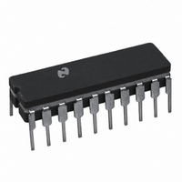
ADC0848BCJ National Semiconductor, ADC0848BCJ Datasheet - Page 13

ADC0848BCJ
Manufacturer Part Number
ADC0848BCJ
Description
IC ADC 8BIT MPU W/MUX OPT 20CDIP
Manufacturer
National Semiconductor
Datasheet
1.ADC0844CCNNOPB.pdf
(24 pages)
Specifications of ADC0848BCJ
Number Of Bits
8
Sampling Rate (per Second)
25k
Data Interface
Parallel
Number Of Converters
1
Power Dissipation (max)
875mW
Voltage Supply Source
Single Supply
Operating Temperature
-40°C ~ 85°C
Mounting Type
Through Hole
Package / Case
20-CDIP (0.300", 7.62mm)
Lead Free Status / RoHS Status
Contains lead / RoHS non-compliant
Other names
*ADC0848BCJ
Available stocks
Company
Part Number
Manufacturer
Quantity
Price
grounding the V
itive voltage to the V
between actual DC input voltage which is necessary to just
cause an output digital code transition from 0000 0000 to
0000 0001 and the ideal ½ LSB value (½ LSB=9.8 mV for
V
4.2 Full-Scale
The full-scale adjustment can be made by applying a differ-
ential input voltage which is 1 ½ LSB down from the desired
analog full-scale voltage range and then adjusting the mag-
nitude of the V
1111 1110 to 1111 1111.
The full-scale adjustment should be made [with the proper
V
which is given by:
REF
IN
(−) voltage applied] by forcing a voltage to the V
=5.000 V
DC
REF
−
).
input and applying a small magnitude pos-
input for a digital output code changing from
+
input. Zero error is the difference
FIGURE 2. Referencing Examples
b) Absolute with a Reduced Span
IN
(+) input
a) Ratiometric
13
4.3 Adjusting for an Arbitrary Analog Input Voltage
Range
If the analog zero voltage of the A/D is shifted away from
ground (for example, to accommodate an analog input signal
which does not go to ground), this new zero reference should
be properly adjusted first. A V
desired zero reference plus ½ LSB (where the LSB is calcu-
lated for the desired analog span, 1 LSB = analog span/256)
is applied to selected “+” input and the zero reference voltage
at the corresponding “−” input should then be adjusted to just
obtain the 00
where V
V
are ground referenced.)
The V
change from FE
procedure.
MIN
=the low end (the offset zero) of the analog range. (Both
REF
MAX
(or V
=the high end of the analog input range and
HEX
CC
HEX
to 01
) voltage is then adjusted to provide a code
501616
to FF
HEX
HEX
code transition.
. This completes the adjustment
501617
IN
(+) voltage which equals this
www.national.com


