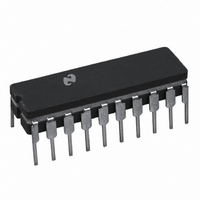
ADC0848BCJ National Semiconductor, ADC0848BCJ Datasheet - Page 3

ADC0848BCJ
Manufacturer Part Number
ADC0848BCJ
Description
IC ADC 8BIT MPU W/MUX OPT 20CDIP
Manufacturer
National Semiconductor
Datasheet
1.ADC0844CCNNOPB.pdf
(24 pages)
Specifications of ADC0848BCJ
Number Of Bits
8
Sampling Rate (per Second)
25k
Data Interface
Parallel
Number Of Converters
1
Power Dissipation (max)
875mW
Voltage Supply Source
Single Supply
Operating Temperature
-40°C ~ 85°C
Mounting Type
Through Hole
Package / Case
20-CDIP (0.300", 7.62mm)
Lead Free Status / RoHS Status
Contains lead / RoHS non-compliant
Other names
*ADC0848BCJ
Available stocks
Company
Part Number
Manufacturer
Quantity
Price
CONVERTER AND MULTIPLEXER CHARACTERISTICS
Maximum Total
Unadjusted Error
Minimum Reference Input Resistance
Maximum Reference Input Resistance
Maximum Common-Mode Input Voltage (Note 9)
Minimum Common-Mode Input Voltage
DC Common-Mode Error
Power Supply Sensitivity
Off Channel Leakage Current
DIGITAL AND DC CHARACTERISTICS
V
V
I
I
V
IN(1)
IN(0)
IN(1)
IN(0)
OUT(1)
Absolute Maximum Ratings
If Military/Aerospace specified devices are required,
please contact the National Semiconductor Sales Office/
Distributors for availability and specifications.
Electrical Characteristics
The following specifications apply for V
limits T
ADC0844BCN, ADC0848BCN, BCV
ADC0844CCN, ADC0848CCN, CCV
ADC0844CCJ (Note 12)
Supply Voltage (V
Voltage
Input Current at Any Pin (Note 3)
Package Input Current (Note 3)
Storage Temperature
Package Dissipation at T
ESD Susceptibility (Note 4)
Lead Temperature
(Soldering, 10 seconds)
, Logical “1” Input Current (Max)
, Logical “0” Input Current (Max)
, Logical “1” Input Voltage (Min)
, Logical “0” Input Voltage (Max)
Logic Control Inputs
At Other Inputs and Outputs
Dual-In-Line Package (Plastic)
, Logical “1” Output Voltage (Min)
A
= T
j
Parameter
= 25°C.
CC
)
A
=25°C
CC
V
(Note 8)
(Note 9)
Differential Mode
V
(Note 10)
On Channel=5V,
Off Channel=0V
On Channel=0V,
Off Channel=5V
V
V
V
V
V
−0.3V to V
REF
CC
CC
CC
IN
IN
CC
= 5 V
−65°C to +150°C
I
I
OUT
OUT
=5.0V
=0V
=5V±5%
=5.25V
=4.75V
=4.75V,
Conditions
=5.00 V
−0.3V to +15V
=−360 μA
=−10 μA
DC
(Notes 1, 2)
unless otherwise specified.Boldface limits apply from T
CC
875 mW
DC
20 mA
260°C
+0.3V
5 mA
800V
6.5V
(Note 5)
−0.005
±1/16
±1/16
0.005
Typ
3
ADC0844BCJ (Note 12)
ADC0844CCJ (Note 12)
2.4
2.4
Operating Conditions
(Notes 1, 2)
* Product/package combination obsolete; shown for reference only.
Supply Voltage (V
Temperature Range
*,
Dual-In-Line Package (Ceramic)
Molded Chip Carrier Package
ADC0844CCN, ADC0848BCN,
ADC0848CCN
ADC0844BCJ *, ADC0844CCJ
ADC0848BCV, ADC0848CCV
V
(Note 6)
Tested
CC
−0.05
Vapor Phase (60 seconds)
Infrared (15 seconds)
Limit
GND
1.1
5.9
±¼
±⅛
2.0
0.8
2.4
4.5
±1
−1
−1
+0.05
1
1
(Note 7)
Design
Limit
CC
)
ADC0848BCN, ADC0848CCN
ADC0848BCV, ADC0848CCV Limit
(Note 5)
−0.005
±1/16
±1/16
0.005
Typ
2.4
2.4
ADC0844CCN
V
(Note 6)
Tested
CC
−0.05
Limit
GND
−0.1
±½
1.2
5.4
±¼
±⅛
0.1
2.0
0.8
2.8
4.6
±1
+0.05 V
MIN
4.5 V
−40°C
to T
T
0°C
MIN
DC
(Note 7)
Design
MAX
CC
−0.05
Limit
GND
www.national.com
≤
≤
≤
±½
1.1
5.9
±¼
±⅛
2.0
0.8
2.4
4.5
to 6.0 V
±1
−1
−1
+0.05
1
1
T
T
T
; all other
A
A
A
≤
≤
≤
300°C
215°C
220°C
70°C
85°C
T
MAX
Units
DC
LSB
LSB
LSB
LSB
LSB
kΩ
kΩ
μA
μA
μA
μA
V
V
V
V
V
V


