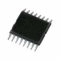
PCA9691TS/1,118 NXP Semiconductors, PCA9691TS/1,118 Datasheet - Page 11

PCA9691TS/1,118
Manufacturer Part Number
PCA9691TS/1,118
Description
IC ADC/DAC 8-BIT I2C 16-TSSOP
Manufacturer
NXP Semiconductors
Type
ADC, DACr
Datasheet
1.PCA9691BS1118.pdf
(31 pages)
Specifications of PCA9691TS/1,118
Package / Case
16-TSSOP
Resolution (bits)
8 b
Data Interface
I²C, Serial
Voltage Supply Source
Single Supply
Voltage - Supply
2.5 V ~ 5.5 V
Operating Temperature
-40°C ~ 85°C
Mounting Type
Surface Mount
Mounting Style
SMD/SMT
Lead Free Status / RoHS Status
Lead free / RoHS Compliant
Sampling Rate (per Second)
-
Lead Free Status / Rohs Status
Lead free / RoHS Compliant
Other names
935283384118
PCA9691TS/1-T
PCA9691TS/1-T
PCA9691TS/1-T
PCA9691TS/1-T
Available stocks
Company
Part Number
Manufacturer
Quantity
Price
Company:
Part Number:
PCA9691TS/1,118
Manufacturer:
NXP
Quantity:
560
NXP Semiconductors
PCA9691_2
Product data sheet
Fig 11. A/D conversion sequence
protocol
SDA
SCL
S
7.4 A/D conversion
1
ADDRESS
The new AOUT value is valid, at the latest, after 8.0 μs so before the rising edge of the 8th
bit of the next transferred byte. Therefore, at the full speed of the I
output is valid under all circumstances between the rising edges of the 8th bit and the
acknowledge bit.
The A/D Converter (ADC) makes use of the successive approximation conversion
technique. The on-chip DAC and a high-gain comparator are used temporarily during an
A/D conversion cycle.
An A/D conversion cycle is always started after sending a valid read mode address to a
PCA9691. The A/D conversion cycle is triggered at the trailing edge of the acknowledge
clock pulse and is executed while transmitting the result of the previous conversion (see
Figure
Once a conversion cycle is triggered, an input voltage sample of the selected channel is
stored on the chip and is converted to the corresponding 8-bit binary code. Samples
picked up from differential inputs are converted to an 8-bit two’s complement code (see
Figure 12
The conversion result is stored in the ADC data register and awaits transmission. If the
auto-increment flag is set the next channel is selected.
2
Fig 10.
V
AOUT
SCL
11).
1
6
8
D/A conversion sequence, example of worst case
and
A
9
7
Figure
conversion of byte 1
1
sampling byte 1
converted byte
> 8T
DATA BYTE 0
8
transmission
of previously
13).
Rev. 02 — 27 January 2010
osc
A
1
< 18T
A
2
9
osc
conversion of byte 2
1
3
DATA BYTE 1
sampling byte 2
transmission
of byte 1
4
5
t
A
s(DAC)
6
9
8-bit A/D and D/A converter
conversion of byte 3
1
sampling byte 3
7
DATA BYTE 2
transmission
2
of byte 2
C-bus, the analog
valid
8
PCA9691
© NXP B.V. 2010. All rights reserved.
A
A
mbl829
1
001aag470
11 of 31
2


