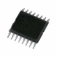
PCA9691TS/1,118 NXP Semiconductors, PCA9691TS/1,118 Datasheet - Page 14

PCA9691TS/1,118
Manufacturer Part Number
PCA9691TS/1,118
Description
IC ADC/DAC 8-BIT I2C 16-TSSOP
Manufacturer
NXP Semiconductors
Type
ADC, DACr
Datasheet
1.PCA9691BS1118.pdf
(31 pages)
Specifications of PCA9691TS/1,118
Package / Case
16-TSSOP
Resolution (bits)
8 b
Data Interface
I²C, Serial
Voltage Supply Source
Single Supply
Voltage - Supply
2.5 V ~ 5.5 V
Operating Temperature
-40°C ~ 85°C
Mounting Type
Surface Mount
Mounting Style
SMD/SMT
Lead Free Status / RoHS Status
Lead free / RoHS Compliant
Sampling Rate (per Second)
-
Lead Free Status / Rohs Status
Lead free / RoHS Compliant
Other names
935283384118
PCA9691TS/1-T
PCA9691TS/1-T
PCA9691TS/1-T
PCA9691TS/1-T
Available stocks
Company
Part Number
Manufacturer
Quantity
Price
Company:
Part Number:
PCA9691TS/1,118
Manufacturer:
NXP
Quantity:
560
NXP Semiconductors
PCA9691_2
Product data sheet
7.7.1 Bit transfer
7.7.2 START and STOP conditions
7.7 Characteristics of the I
It is recommended that if the I
frequency by half (see the definition of the control byte in
If pin EXT is connected to V
state allowing to feed an external clock signal to the OSC input. The frequency of the
external clock must be in the specified range.
The I
The two lines are a Serial DAta Line (SDA) and a Serial Clock Line (SCL). Both lines are
connected to a positive supply via a pull-up resistor. Data transfer is initiated only when
the bus is not busy.
One data bit is transferred during each clock pulse. The data on the SDA line remains
stable during the HIGH period of the clock pulse as changes in the data line at this time
are interpreted as control signals (see
Both data and clock lines remain HIGH when the bus is not busy.
A HIGH-to-LOW transition of the data line while the clock is HIGH is defined as the START
condition (S).
A LOW-to-HIGH transition of the data line while the clock is HIGH is defined as the STOP
condition (P) (see
Fig 14. Bit transfer
Fig 15. Definition of start and stop condition
2
C-bus is for bidirectional, two-line communication between different IC or modules.
SDA
SCL
START condition
SDA
SCL
Figure
S
Rev. 02 — 27 January 2010
15).
DD
2
2
C-bus speed f
C-bus
the oscillator output OSC is switched to a high-impedance
data valid
data line
stable;
Figure
SCL
14).
allowed
change
of data
≤ 400 kHz, you must reduce the oscillator
Figure
8-bit A/D and D/A converter
STOP condition
6).
mbc621
P
PCA9691
© NXP B.V. 2010. All rights reserved.
mbc622
SDA
SCL
14 of 31


