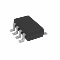
AD5228BUJZ10-R2 Analog Devices Inc, AD5228BUJZ10-R2 Datasheet - Page 13

AD5228BUJZ10-R2
Manufacturer Part Number
AD5228BUJZ10-R2
Description
IC DGTL POT 10K UP/DN TSOT23-8
Manufacturer
Analog Devices Inc
Datasheet
1.AD5228BUJZ10-RL7.pdf
(20 pages)
Specifications of AD5228BUJZ10-R2
Taps
32
Resistance (ohms)
10K
Number Of Circuits
1
Temperature Coefficient
35 ppm/°C Typical
Memory Type
Volatile
Interface
Up/Down Counter
Voltage - Supply
2.7 V ~ 5.5 V
Operating Temperature
-40°C ~ 105°C
Mounting Type
Surface Mount
Package / Case
TSOT-23-8, TSOT-8
Resistance In Ohms
10K
End To End Resistance
10kohm
Track Taper
Linear
No. Of Steps
32
Resistance Tolerance
± 20%
Supply Voltage Range
2.7V To 5.5V
Control Interface
Pushbutton
No. Of Pots
Single
Lead Free Status / RoHS Status
Lead free / RoHS Compliant
For Use With
EVAL-AD5228EBZ - BOARD EVAL FOR AD5228 DGTL POT
Lead Free Status / Rohs Status
Compliant
Potentiometer Mode Operation
If all three terminals are used, the operation is called potenti-
ometer mode. The most common configuration is the voltage
divider operation as shown in Figure 36.
The change of V
maximum or minimum scale has not been reached during
operation. If the effect of wiper resistance is ignored, the
transfer functions can be simplified as
Unlike in rheostat mode operation where the absolute tolerance
is high, potentiometer mode operation yields an almost ratio-
metric function of PU /32 or PD /32 with a relatively small error
contributed by the R
almost canceled. Although the thin film step resistor R
CMOS switch resistance, R
coefficients, the ratiometric adjustment also reduces the overall
temperature coefficient effect to 5 ppm/°C except at low value
codes where R
Potentiometer mode operations include an op amp input and
feedback resistors network and other voltage scaling applications.
The A, W, and B terminals can be input or output terminals and
have no polarity constraint provided that |V
do not exceed V
Δ
Δ
V
V
WB
WB
=
=
Figure 36. Potentiometer Mode Configuration
+
+
W
PU
PD
32
32
DD
WB
dominates.
-to-GND.
V
V
is known provided that the AD5228
A
W
A
V
term. The tolerance effect is, therefore,
I
W
, have very different temperature
A
B
W
V
C
AB
|, |V
WA
|, and |V
S
and
Rev. A | Page 13 of 20
WB
(5)
(6)
|
CONTROLLING INPUTS
All PU and PD inputs are protected with a Zener ESD structure
as shown in
PU and PD pins are usually connected to pushbutton tactile
switches for manual operation, but the AD5228 can also be
controlled digitally. It is recommended to add external
MOSFETs or transistors that simplify the logic controls.
TERMINAL VOLTAGE OPERATION RANGE
The AD5228 is designed with internal ESD diodes for
protection. These diodes also set the voltage boundary of the
terminal operating voltages. Positive signals present on
Terminal A, B, or W that exceed V
forward-biased diode. There is no polarity constraint between
V
than GND.
2N7002
UP
A
, V
N1
W
, and V
Figure 39. Maximum Terminal Voltages Set by V
Figure 37. Equivalent ESD Protection in PU and PD Pins
DOWN
2N7002
Figure 38. Digital Control with External MOSFETs
Figure 37
N2
B
, but they cannot be higher than V
V
PU
PD
DD
PU
100kΩ
.
R1
V
DD
R2
SCAN DETECT
DEBOUNCE
DEBOUNCER
STEP/AUTO
DECODE
CONTROL
DISCRETE
ADAPTIVE
UP/DOWN
AND
LOGIC
CKT
DD
are clamped by the
V
A
W
B
GND
DD
PRE
D
E
C
O
D
E
SCALE PRESET
ZERO- OR MID-
DD
and GND
DD
AD5228
or lower
AD5228
GND
A
W
B


