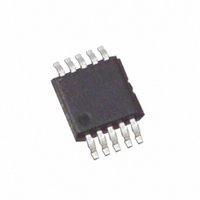
ISL95710WIU10Z Intersil, ISL95710WIU10Z Datasheet - Page 5

ISL95710WIU10Z
Manufacturer Part Number
ISL95710WIU10Z
Description
IC XDCP 128-TAP 10KOHM 10-MSOP
Manufacturer
Intersil
Series
XDCP™r
Datasheet
1.ISL95710WIU10Z-T.pdf
(10 pages)
Specifications of ISL95710WIU10Z
Taps
128
Resistance (ohms)
10K
Number Of Circuits
1
Temperature Coefficient
50 ppm/°C Typical
Memory Type
Non-Volatile
Interface
Up/Down (3-Wire)
Voltage - Supply
2.7 V ~ 5.5 V
Operating Temperature
-40°C ~ 85°C
Mounting Type
Surface Mount
Package / Case
10-MSOP, Micro10™, 10-uMAX, 10-uSOP
Resistance In Ohms
10K
Number Of Elements
1
# Of Taps
128
Resistance (max)
10KOhm
Interface Type
Serial (3-Wire)
Single Supply Voltage (typ)
-3.3V
Dual Supply Voltage (typ)
Not RequiredV
Single Supply Voltage (min)
-2.7V
Single Supply Voltage (max)
-5.5V
Dual Supply Voltage (min)
Not RequiredV
Dual Supply Voltage (max)
Not RequiredV
Operating Temp Range
-40C to 85C
Operating Temperature Classification
Industrial
Mounting
Surface Mount
Pin Count
10
Lead Free Status / RoHS Status
Lead free / RoHS Compliant
AC Electrical Specifications
NOTES:
Symbol Table
10. RDNL = (R
12.
13. This parameter is not 100% tested.
14. t
11. RINL = [R
1. Typical values are for T
2. LSB: [V(R
3. ZS error = (V(R
4. FS error = [V(R
5. DNL = [V(R
6. INL = V(R
7.
8. MI =
9. Roffset = R
incremental voltage when changing from one tap to an adjacent tap.
for i = 16 to 120 decimal. Max ( ) is the maximum value of the wiper voltage and Min ( ) is the minimum value of the wiper voltage over the
temperature range.
Roffset = R
for i = 16 to 127, T = -40°C to +85°C. Max ( ) is the maximum value of the resistance and Min ( ) is the minimum value of the resistance over
the temperature range.
the self-timed internal non-volatile write cycle. No CS or INC changes should be allowed.
TC V
CPHS
TC R
SYMBOL
WAVEFORM
t
t
R
CYC
t
|
IW
R
, t
=
is the minimum cycle time to be allowed for any non-volatile Write by the user. It is the time from a valid STORE condition to the end of
=
127
F
----------------------------------------------------------------------------------------------x
[
--------------------------------------------------------------- -
[
W
W
Max V RW
i
Max Ri
– (MI • i) – R
[
i
0
127
W
Max V RW
– R
)
)
Max Ri
– R
/MI, when measuring between RW and RL.
127
i
)
– (i • LSB – V(R
i
(
/MI, when measuring between RW and RH.
0
(
W
– V(R
W
i-1
|
(
– V(R
(
)
)
(
/127. R
)/MI -1, for i = 16 to 127.
INC to R
INC cycle time
INC input rise and fall time
0
127
)
(
– V-)/LSB.
+
) Min Ri
W
May change from Low to High
May change from High to Low
–
Must be steady
Don’t Care: Changes Allowed
N/A
Min Ri
INPUTS
– V+]/LSB.
W
) i
)
A
0
i-1
) i
)
)
127
]/MI, for i = 16 to 127.
0
= +25°C and 3.3V supply voltage.
+
) Min V RW
]/LSB-1, for i = 1 to 127. i is the DCP register setting.
(
]/127. V(R
W
–
Min V RW
(
and R
change
5
W
)
] 2 ⁄
)
(
)
]
0
(
)/LSB for i = 1 to 127.
(
×
0
(
V
---------------- -
125°C
W
are the measured resistances for the DCP register set to 7F hex and 00 hex respectively.
PARAMETER
10
CC
)
) i
127
) i
6
)
] 2 ⁄
= 5V ±10%, T
)
and V(R
---------------- -
125°C
10 6
W
)
0
A
are V(R
= Full Operating Temperature Range unless otherwise stated (Continued)
OUTPUTS
Will be steady
Will change from Low to High
Will change from High to Low
Changing: State Not Known
Center Line is High Impedance
ISL95710
W
) for the DCP register set to 7F hex and 00 hex respectively. LSB is the
MIN
2
TYP (Note 1)
100
MAX
500
500
August 31, 2006
UNIT
µs
µs
µs
FN8240.3


