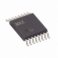
DS1881E-050+ Maxim Integrated Products, DS1881E-050+ Datasheet - Page 15

DS1881E-050+
Manufacturer Part Number
DS1881E-050+
Description
IC POT DIGIT DL NV 50K 16TSSOP
Manufacturer
Maxim Integrated Products
Datasheet
1.DS1881Z-050.pdf
(16 pages)
Specifications of DS1881E-050+
Taps
64
Resistance (ohms)
45K
Number Of Circuits
2
Temperature Coefficient
750 ppm/°C Typical
Memory Type
Non-Volatile
Interface
I²C, 2-Wire Serial
Voltage - Supply
2.7 V ~ 5.5 V
Operating Temperature
-40°C ~ 85°C
Mounting Type
Surface Mount
Package / Case
16-TSSOP
Resistance In Ohms
45K
Lead Free Status / RoHS Status
Lead free / RoHS Compliant
Byte Write: A byte write consists of 8 bits of informa-
tion transferred from the master to the slave (most sig-
nificant bit first) plus a 1-bit acknowledgement from the
slave to the master. The 8 bits transmitted by the mas-
ter are done according to the bit write definition and the
acknowledgement is read using the bit read definition.
Byte Read: A byte read is an 8-bit information transfer
from the slave to the master plus a 1-bit ACK or NACK
from the master to the slave. The 8 bits of information
that are transferred (most significant bit first) from the
slave to the master are read by the master using the bit
read definition, and the master transmits an ACK using
the bit write definition to receive additional data bytes.
The master must NACK the last byte read to terminate
communication so the slave will return control of SDA to
the master.
Slave Address Byte: Each slave on the I
responds to a slave addressing byte sent immediately
following a START condition. The slave address byte
(Figure 5) contains the slave address in the most signif-
icant 7 bits and the R/W bit in the least significant bit.
The DS1881’s slave address is 0101 A2 A1 A0 (binary),
where A2, A1, and A0 are the values of the address
pins. The address pins allow the device to respond to
one of eight possible slave addresses. By writing the
correct slave address with R/W = 0, the master indi-
cates it will write data to the slave. If R/W = 1, the mas-
ter will read data from the slave. If an incorrect slave
address is written, the DS1881 will assume the master is
communicating with another I
communications until the next START condition is sent.
Writing a Single Byte to a Slave: The master must
generate a START condition, write the slave address
byte (R/W = 0), write the byte of data, and generate a
STOP condition. The master must read the slave’s
acknowledgement during all byte write operations.
Figure 5. DS1881’s Slave Address Byte
MSB
0
Dual NV Audio Taper Digital Potentiometer
1
0
7-BIT SLAVE
ADDRESS
1
A2
A2, A1, AND A0
2
PIN VALUES
I
C device and ignore the
2
C Communication
A1
A0
____________________________________________________________________
READ OR WRITE
DETERMINES
FUNCTION
R/W
LSB
2
C bus
Writing Multiple Bytes to a Slave: To write multiple
bytes to a slave, the master generates a START condi-
tion, writes the slave address byte (R/W = 0), writes the
desired number of data bytes and generates a STOP
condition. The DS1881 is capable of writing both poten-
tiometer wiper settings and the Configuration Register
with a single write transaction.
Acknowledge Polling: Any time an EEPROM location
is written, the DS1881 requires the EEPROM write time
(t
the byte of data to EEPROM. During the EEPROM write
time, the device will not acknowledge its slave address
because it is busy. It is possible to take advantage of
that phenomenon by repeatedly addressing the
DS1881, which allows the next page to be written as
soon as the DS1881 is ready to receive the data. The
alternative to acknowledge polling is to wait for a maxi-
mum period of t
again to the device.
EEPROM Write Cycles: When EEPROM writes occur to
the memory, the DS1881 will write to all three EEPROM
memory locations, even if only a single byte was modi-
fied. Because all three bytes are written, the bytes that
were not modified during the write transaction are still
subject to a write cycle. This can result in all three bytes
being worn out over time by writing a single byte repeat-
edly. The DS1881’s EEPROM write cycles are specified in
the NV Memory Characteristics table. The specification
shown is at the worst-case temperature. If zero-crossing
detection is enabled, EEPROM write cycles cannot begin
until after the zero-crossing detection is complete.
Reading a Single Byte from a Slave: To read a single
byte from the slave, the master generates a START con-
dition, writes the slave address byte with R/W = 1, reads
the data byte with a NACK to indicate the end of the
transfer, and generates a STOP condition. When a single
byte is read, it will always be the Potentiometer 0 value.
Reading Multiple Bytes from a Slave: The read oper-
ation can be used to read multiple bytes with a single
transfer. When reading bytes from the slave, the master
simply ACKs the data byte if it desires to read another
byte before terminating the transaction. After the mas-
ter reads the last byte, it NACKs to indicate the end of
the transfer and generates a STOP condition. The first
byte read will be the Potentiometer 0 Wiper Setting. The
next byte will be the Potentiometer 1 Wiper Setting. The
third byte is the Configuration Register byte. If an ACK
is issued by the master following the Configuration
Register byte, then the DS1881 will send the
Potentiometer 0 Wiper Setting again. This round robin
reading will occur as long as each byte read is followed
by an ACK from the master.
W
) after the STOP condition to write the contents of
W
to elapse before attempting to write
15


