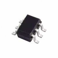
AD5246BKS5-R2 Analog Devices Inc, AD5246BKS5-R2 Datasheet - Page 13

AD5246BKS5-R2
Manufacturer Part Number
AD5246BKS5-R2
Description
IC POT DGTL 5K 128POS SC70-6
Manufacturer
Analog Devices Inc
Datasheet
1.AD5246BKSZ50-RL7.pdf
(16 pages)
Specifications of AD5246BKS5-R2
Rohs Status
RoHS non-compliant
Taps
128
Resistance (ohms)
5K
Number Of Circuits
1
Temperature Coefficient
45 ppm/°C Typical
Memory Type
Volatile
Interface
I²C, 2-Wire Serial
Voltage - Supply
2.7 V ~ 5.5 V
Operating Temperature
-40°C ~ 125°C
Mounting Type
Surface Mount
Package / Case
SC-70-6, SC-88, SOT-363
Resistance In Ohms
5K
Number Of Elements
1
# Of Taps
128
Resistance (max)
5KOhm
Power Supply Requirement
Single
Interface Type
Serial (2-Wire/I2C)
Single Supply Voltage (typ)
3/5V
Dual Supply Voltage (typ)
Not RequiredV
Single Supply Voltage (min)
2.7V
Single Supply Voltage (max)
5.5V
Dual Supply Voltage (min)
Not RequiredV
Dual Supply Voltage (max)
Not RequiredV
Operating Temp Range
-40C to 125C
Operating Temperature Classification
Automotive
Mounting
Surface Mount
Pin Count
6
Lead Free Status / RoHS Status
Not Compliant
Other names
AD5246BKS5-R2TR
Available stocks
Company
Part Number
Manufacturer
Quantity
Price
Company:
Part Number:
AD5246BKS5-R2
Manufacturer:
ANALOG
Quantity:
250
OPERATION
The AD5246 is a 128-position, digitally controlled variable
resistor (VR) device.
PROGRAMMING THE VARIABLE RESISTOR
Rheostat Operation
The nominal resistance of the RDAC between Terminal A
and Terminal B is available in 5 kΩ, 10 kΩ, 50 kΩ, and 100 kΩ.
The final two or three digits of the part number determine
the nominal resistance value, that is, 10 kΩ = 10, 50 kΩ = 50.
The nominal resistance (R
accessed by the wiper terminal. The 7-bit data in the RDAC
latch is decoded to select one of the 128 possible settings.
The general equation determining the digitally programmed
output resistance between W and B is
where:
D is the decimal equivalent of the binary code loaded in the
7-bit RDAC register.
R
R
of each internal switch.
Note that in the zero-scale condition, there is a relatively small
finite wiper resistance. Care should be taken to limit the current
flow between W and B in this state to a maximum pulse current
of no more than 20 mA. Otherwise, degradation or possible
destruction of the internal switch contact can occur.
Typical device-to-device matching is process lot dependent and
may vary by up to ±30%. Since the resistance element is proc-
essed in thin-film technology, the temperature coefficient of
R
AB
W
AB
is the wiper resistance contributed by the on resistance
is the end-to-end resistance.
is only 45 ppm/°C.
R
WB
(
D
)
=
Figure 29. AD5246 Equivalent RDAC Circuit
128
D
D6
D5
D4
D3
D2
D1
D0
DECODER
LATCH
RDAC
AND
×
R
AB
+
R
R
R
AB
S
S
S
2
) of the VR has 128 contact points
×
R
W
Ax
Wx
Bx
(1)
Rev. B | Page 13 of 16
I
The first byte of the AD5246 is a slave address byte (see Table 6
and Table 7). It has a 7-bit slave address and an R/ W bit. The
seven MSBs of the slave address are 0101110 followed by 0
for a write command or 1 to place the device in read mode.
The 2-wire I
1.
2.
3.
4.
2
C COMPATIBLE 2-WIRE SERIAL BUS
The master initiates data transfer by establishing a START
condition, which is when a high-to-low transition on the
SDA line occurs while SCL is high (see Figure 27). The
following byte is the slave address byte, which consists of
the 7-bit slave address followed by an R/ W bit (this bit
determines whether data will be read from or written to
the slave device).
The slave whose address corresponds to the transmitted
address responds by pulling the SDA line low during the
ninth clock pulse (this is termed the acknowledge bit).
At this stage, all other devices on the bus remain idle while
the selected device waits for data to be written to or read
from its serial register. If the R/ W bit is high, the master
reads from the slave device. Conversely, if the R/ W bit is
low, the master writes to the slave device.
In write mode, after acknowledgement of the slave address
byte, the next byte is the data byte. Data is transmitted over
the serial bus in sequences of nine clock pulses (eight data
bits followed by an acknowledge bit). The transitions on
the SDA line must occur during the low period of SCL and
remain stable during the high period of SCL (see Table 6).
In read mode, after acknowledgment of the slave address
byte, data is received over the serial bus in sequences of
nine clock pulses (a slight difference from the write mode
where eight data bits are followed by an acknowledge bit).
Similarly, the transitions on the SDA line must occur
during the low period of SCL and remain stable during
the high period of SCL (see Figure 28).
When all data bits have been read or written, a STOP
condition is established by the master. A STOP condition
is defined as a low-to-high transition on the SDA line while
SCL is high. In write mode, the master pulls the SDA line
high during the tenth clock pulse to establish a STOP
condition (see Figure 27). In read mode, the master issues
a No Acknowledge for the ninth clock pulse (that is, the
SDA line remains high). The master then brings the SDA
line low before the tenth clock pulse, which goes high to
establish a STOP condition (see Figure 28).
2
C serial bus protocol operates as follows:
AD5246


