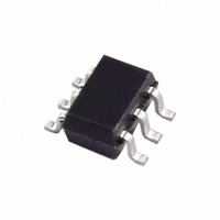
AD5246BKS5-R2 Analog Devices Inc, AD5246BKS5-R2 Datasheet - Page 14

AD5246BKS5-R2
Manufacturer Part Number
AD5246BKS5-R2
Description
IC POT DGTL 5K 128POS SC70-6
Manufacturer
Analog Devices Inc
Datasheet
1.AD5246BKSZ50-RL7.pdf
(16 pages)
Specifications of AD5246BKS5-R2
Rohs Status
RoHS non-compliant
Taps
128
Resistance (ohms)
5K
Number Of Circuits
1
Temperature Coefficient
45 ppm/°C Typical
Memory Type
Volatile
Interface
I²C, 2-Wire Serial
Voltage - Supply
2.7 V ~ 5.5 V
Operating Temperature
-40°C ~ 125°C
Mounting Type
Surface Mount
Package / Case
SC-70-6, SC-88, SOT-363
Resistance In Ohms
5K
Number Of Elements
1
# Of Taps
128
Resistance (max)
5KOhm
Power Supply Requirement
Single
Interface Type
Serial (2-Wire/I2C)
Single Supply Voltage (typ)
3/5V
Dual Supply Voltage (typ)
Not RequiredV
Single Supply Voltage (min)
2.7V
Single Supply Voltage (max)
5.5V
Dual Supply Voltage (min)
Not RequiredV
Dual Supply Voltage (max)
Not RequiredV
Operating Temp Range
-40C to 125C
Operating Temperature Classification
Automotive
Mounting
Surface Mount
Pin Count
6
Lead Free Status / RoHS Status
Not Compliant
Other names
AD5246BKS5-R2TR
Available stocks
Company
Part Number
Manufacturer
Quantity
Price
Company:
Part Number:
AD5246BKS5-R2
Manufacturer:
ANALOG
Quantity:
250
AD5246
A repeated write function gives the user flexibility to update the
RDAC output a number of times after addressing the part only
once. For example, after the RDAC has acknowledged its slave
address in write mode, the RDAC output updates on each succes-
sive byte. If different instructions are needed, the write/read mode
has to start again with a new slave address and data byte.
Similarly, a repeated read function of the RDAC is also allowed.
LEVEL SHIFTING FOR BIDIRECTIONAL INTERFACE
While most legacy systems may be operated at one voltage,
a new component may be optimized at another. When two
systems operate the same signal at two different voltages, proper
level shifting is needed. For instance, one can use a 1.8 V
E
shifting scheme is needed to enable a bidirectional communi-
cation so that the setting of the digital potentiometer can be
stored to and retrieved from the E
one of the implementations. M1 and M2 can be any N channel
signal FETs, or if V
threshold FETs such as the FDV301N.
ESD PROTECTION
All digital inputs are protected with a series input resistor
and parallel Zener ESD structures, as shown in Figure 31.
This applies to the digital input pins SDA and SCL.
TERMINAL VOLTAGE OPERATING RANGE
The AD5246 V
conditions for proper 3-terminal digital potentiometer
operation. Supply signals present on Terminal B and
Terminal W that exceed V
the internal forward biased diodes (see Figure 32).
2
PROM to interface with a 5 V digital potentiometer. A level
V
SDA1
SCL1
DD1
Figure 30. Level Shifting for Operation at Different Potentials
= 1.8V
E
2
PROM
1.8V
DD
Figure 31. ESD Protection of Digital Pins
R
P
and GND power supply defines the boundary
DD
falls below 2.5 V, M1 and M2 can be low
R
P
S
340Ω
DD
G
M1
GND
or GND are clamped by
D
S
LOGIC
2
G
M2
PROM. Figure 30 shows
D
R
P
AD5246
R
P
5V
V
DD2 =
5V
SDA2
SCL2
Rev. B | Page 14 of 16
MAXIMUM OPERATING CURRENT
At low code values, the user should be aware that due to low
resistance values, the current through the RDAC may exceed
the 5 mA limit. In Figure 33, a 5 V supply is placed on the
wiper, and the current through Terminal W and Terminal B is
plotted with respect to code. A line is also drawn denoting the
5 mA current limit. Note that at low code values (particularly
for the 5 kΩ and 10 kΩ options), the current level increases
significantly. Care should be taken to limit the current flow
between W and B in this state to a maximum continuous
current of 5 mA and a maximum pulse current of no more than
20 mA. Otherwise, degradation or possible destruction of the
internal switch contacts can occur.
POWER-UP SEQUENCE
Since the ESD protection diodes limit the voltage compliance
at Terminal B and Terminal W (see Figure 32), it is important
to power V
and Terminal W; otherwise, the diode is forward biased such
that V
the user’s circuit. The ideal power-up sequence is in the follow-
ing order: GND, V
relative order of powering V
is not important, providing they are powered after V
DD
0.01
100
Figure 32. Maximum Terminal Voltages Set by V
0.1
10
1
is powered unintentionally and may affect the rest of
0
DD
/GND before applying any voltage to Terminal B
16
Figure 33. Maximum Operating Current
DD
, digital inputs, and then V
32
5mA CURRENT LIMIT
48
CODE (Decimal)
B
and V
64
W
R
and the digital inputs
AB
80
= 10k Ω
R
AB
V
B
W
GND
DD
= 100k Ω
R
96
R
AB
DD
AB
B
/V
= 5k Ω
and GND
= 50k Ω
112
W
. The
DD
/GND.
128


