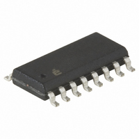
X9428WS16I-2.7 Intersil, X9428WS16I-2.7 Datasheet - Page 14

X9428WS16I-2.7
Manufacturer Part Number
X9428WS16I-2.7
Description
IC DIGITAL POT 10K 64TP 16SOIC
Manufacturer
Intersil
Series
XDCP™r
Datasheet
1.X9428WS16.pdf
(21 pages)
Specifications of X9428WS16I-2.7
Taps
64
Resistance (ohms)
10K
Number Of Circuits
1
Temperature Coefficient
300 ppm/°C Typical
Memory Type
Non-Volatile
Interface
I²C, 2-Wire Serial
Voltage - Supply
2.7 V ~ 5.5 V
Operating Temperature
-40°C ~ 85°C
Mounting Type
Surface Mount
Package / Case
16-SOIC (0.300", 7.5mm Width)
Resistance In Ohms
10K
Lead Free Status / RoHS Status
Contains lead / RoHS non-compliant
Available stocks
Company
Part Number
Manufacturer
Quantity
Price
Company:
Part Number:
X9428WS16I-2.7
Manufacturer:
Intersil
Quantity:
125
D.C. OPERATING CHARACTERISTICS (Over the recommended operating conditions unless otherwise specified.)
Notes: (1) Absolute linearity is utilized to determine actual wiper voltage versus expected voltage as determined by wiper position when used as a
ENDURANCE AND DATA RETENTION
CAPACITANCE
POWER-UP TIMING
POWER-UP AND POWER-DOWN
There are no restrictions on the power-up or power-down sequencing of the bias supplies V
that all three supplies reach their final values within 1msec of each other. However, at all times, the voltages on the
potentiometer pins must be less than V+ and more than V-. The recall of the wiper position from nonvolatile memory
is not in effect until all supplies reach their final value.
Notes: (5) This parameter is periodically sampled and not 100% tested
Symbol
I
I
Symbol
V
V
t
CC1
CC2
I
I
V
Symbol
C
t
SB
I
LO
R
C
t
LI
OL
PUW
PUR
IH
IL
I/O
V
IN
(2) Relative linearity is utilized to determine the actual change in voltage between two successive tap positions when used as a potentiom-
(3) MI = RTOT/63 or (R
(4) Max. = all four arrays cascaded together, Typical = individual array resolutions.
(6) t
(7) Sample tested only.
CC
(5)
(5)
(6)
potentiometer.
eter. It is a measure of the error in step size.
(6)
instruction can be issued. These parameters are periodically sampled and not 100% tested.
Minimum endurance
(7)
PUR
V
(nonvolatile write)
V
(move wiper, write, read)
V
Input leakage current
Output leakage current
Input HIGH voltage
Input LOW voltage
Output LOW voltage
Data retention
CC
CC
CC
Parameter
and t
Input/output capacitance (SDA)
Input capacitance (A0, A1, A2, A3, and SCL)
supply current
supply current
current (standby)
Power-up to initiation of read operation
Power-up to initiation of write operation
V
PUW
CC
Parameter
Power-up ramp rate
are the delays required from the time the third (last) power supply (V
H
14
- R
L
)/63, single pot
Parameter
Test
V
100,000
CC
Min.
100
Min.
-0.5
x 0.7
X9428
Typ.
Limits
V
V
CC
CC
Max.
100
0.4
10
10
Min.
1
1
0.2
x 0.5
x 0.1
Max.
8
6
Data changes per bit per register
Unit
CC
mA
µA
µA
µA
µA
V
V
V
, V+ or V-) is stable until the specific
Typ.
I
f
Other Inputs = V
f
Other Inputs = V
SCL = SDA = V
V
V
SCL
SCL
OL
Years
Unit
IN
OUT
Unit
pF
pF
= 3mA
= V
= 400kHz, SDA = Open,
= 400kHz, SDA = Open,
= V
Test Conditions
SS
CC
SS
Max.
to V
50
, V+, and V- provided
1
5
to V
Test Conditions
CC
CC
SS
SS
CC
V
, Addr. = V
V
I/O
IN
= 0V
= 0V
V/msec
Unit
April 26, 2006
ms
ms
FN8197.1
SS


