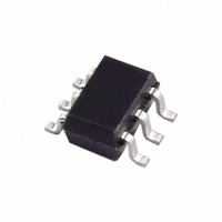
AD5641AKSZ-500RL7 Analog Devices Inc, AD5641AKSZ-500RL7 Datasheet - Page 14

AD5641AKSZ-500RL7
Manufacturer Part Number
AD5641AKSZ-500RL7
Description
IC DAC 14BIT V-OUT SC70-6
Manufacturer
Analog Devices Inc
Series
nanoDAC™r
Datasheet
1.AD5641AKSZ-500RL7.pdf
(20 pages)
Specifications of AD5641AKSZ-500RL7
Data Interface
SPI™
Settling Time
6µs
Number Of Bits
14
Number Of Converters
1
Voltage Supply Source
Single Supply
Power Dissipation (max)
550µW
Operating Temperature
-40°C ~ 125°C
Mounting Type
Surface Mount
Package / Case
SC-70-6, SC-88, SOT-363
Resolution (bits)
14bit
Sampling Rate
1.7MSPS
Input Channel Type
Serial
Supply Voltage Range - Analog
2.7V To 5.5V
Supply Current
75µA
Digital Ic Case Style
SC-70
Number Of Channels
1
Resolution
14b
Conversion Rate
1.7MSPS
Interface Type
Serial (3-Wire, SPI, QSPI, Microwire)
Single Supply Voltage (typ)
3.3/5V
Dual Supply Voltage (typ)
Not RequiredV
Architecture
Resistor-String
Power Supply Requirement
Single
Output Type
Voltage
Integral Nonlinearity Error
±16LSB
Single Supply Voltage (min)
2.7V
Single Supply Voltage (max)
5.5V
Dual Supply Voltage (min)
Not RequiredV
Dual Supply Voltage (max)
Not RequiredV
Operating Temp Range
-40C to 125C
Operating Temperature Classification
Automotive
Mounting
Surface Mount
Pin Count
6
Package Type
SC-70
Lead Free Status / RoHS Status
Lead free / RoHS Compliant
Lead Free Status / RoHS Status
Lead free / RoHS Compliant, Lead free / RoHS Compliant
Other names
AD5641AKSZ-500RL7TR
AD5641AKSZ500RLTR
AD5641AKSZ500RLTR
AD5641AKSZ500RLTR
AD5641AKSZ500RLTR
AD5641
POWER-ON RESET
The AD5641 contains a power-on reset circuit that controls the
output voltage during power-up. The DAC register is filled with
0s and the output voltage is 0 V. It remains there until a valid
write sequence is made to the DAC. This is useful in applica-
tions in which it is important to know the state of the DAC
output while it is in the process of powering up.
POWER-DOWN MODES
The AD5641 has four separate modes of operation. These
modes are software programmable by setting two bits (DB15
and DB14) in the control register. Table 6 shows how the state
of the bits corresponds to the operating mode of the device.
Table 6. Operating Modes for the AD5641
DB15
0
0
1
1
When both bits are set to 0, the part has normal power
consumption of 100 μA maximum at 5 V. However, for the
three power-down modes, the supply current falls to typically
0.2 μA at 3 V.
SCLK
SYNC
SDIN
DB14
0
1
0
1
SYNC HIGH BEFORE 16
DB15
INVALID WRITE SEQUENCE:
DB15 (MSB)
PD1
PD0
Operating Mode
Normal operation
Power-down mode:
1 kΩ to GND
100 kΩ to GND
Three-state
TH
D13
0
0
1
1
FALLING EDGE
DB0
0
1
0
1
D12
NORMAL OPERATION
1 kΩ TO GND
100 kΩ TO GND
THREE-STATE
D11
D10
Figure 34. Input Register Contents
Figure 35. SYNC Interrupt Facility
D9
POWER-DOWN MODES
Rev. C | Page 14 of 20
D8
DATA BITS
D7
Not only does the supply current fall, but the output stage is
also internally switched from the output of the amplifier to a
resistor network of known values. This has the advantage that
the output impedance of the part is known while the part is in
power-down mode. There are three different options: the
output is connected internally to GND through either a 1 kΩ
resistor or a 100 kΩ resistor, or the output is left open-circuited
(three-stated). Figure 36 shows the output stage.
The bias generator, output amplifier, resistor string, and other
associated linear circuitry are all shut down when power-down
mode is activated. However, the contents of the DAC register
are unaffected when in power-down. The time to exit power-
down is typically 13 μs for V
See Figure 28 for a plot.
D6
VALID WRITE SEQUENCE, OUTPUT UPDATES
D5
STRING DAC
DB16
RESISTOR
ON THE 16
D4
Figure 36. Output Stage During Power-Down
D3
TH
FALLING EDGE
D2
POWER-DOWN
AMPLIFIER
CIRCUITRY
DD
DB0
D1
DB0 (LSB)
= 5 V and 16 μs for V
D0
NETWORK
RESISTOR
V
DD
OUT
= 3 V.


