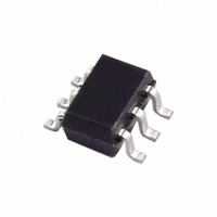
AD5641AKSZ-500RL7 Analog Devices Inc, AD5641AKSZ-500RL7 Datasheet - Page 15

AD5641AKSZ-500RL7
Manufacturer Part Number
AD5641AKSZ-500RL7
Description
IC DAC 14BIT V-OUT SC70-6
Manufacturer
Analog Devices Inc
Series
nanoDAC™r
Datasheet
1.AD5641AKSZ-500RL7.pdf
(20 pages)
Specifications of AD5641AKSZ-500RL7
Data Interface
SPI™
Settling Time
6µs
Number Of Bits
14
Number Of Converters
1
Voltage Supply Source
Single Supply
Power Dissipation (max)
550µW
Operating Temperature
-40°C ~ 125°C
Mounting Type
Surface Mount
Package / Case
SC-70-6, SC-88, SOT-363
Resolution (bits)
14bit
Sampling Rate
1.7MSPS
Input Channel Type
Serial
Supply Voltage Range - Analog
2.7V To 5.5V
Supply Current
75µA
Digital Ic Case Style
SC-70
Number Of Channels
1
Resolution
14b
Conversion Rate
1.7MSPS
Interface Type
Serial (3-Wire, SPI, QSPI, Microwire)
Single Supply Voltage (typ)
3.3/5V
Dual Supply Voltage (typ)
Not RequiredV
Architecture
Resistor-String
Power Supply Requirement
Single
Output Type
Voltage
Integral Nonlinearity Error
±16LSB
Single Supply Voltage (min)
2.7V
Single Supply Voltage (max)
5.5V
Dual Supply Voltage (min)
Not RequiredV
Dual Supply Voltage (max)
Not RequiredV
Operating Temp Range
-40C to 125C
Operating Temperature Classification
Automotive
Mounting
Surface Mount
Pin Count
6
Package Type
SC-70
Lead Free Status / RoHS Status
Lead free / RoHS Compliant
Lead Free Status / RoHS Status
Lead free / RoHS Compliant, Lead free / RoHS Compliant
Other names
AD5641AKSZ-500RL7TR
AD5641AKSZ500RLTR
AD5641AKSZ500RLTR
AD5641AKSZ500RLTR
AD5641AKSZ500RLTR
MICROPROCESSOR INTERFACING
AD5641 to ADSP-2101 Interface
Figure 37 shows a serial interface between the AD5641 and the
ADSP-2101. The ADSP-2101 should be set up to operate in
SPORT transmit alternate framing mode. The ADSP-2101
SPORT is programmed through the SPORT control register and
should be configured as follows: internal clock operation, active
low framing, and 16-bit word length. Transmission is initiated
by writing a word to the Tx register after the SPORT is enabled.
AD5641 to 68HC11/68L11 Interface
Figure 38 shows a serial interface between the AD5641 and the
68HC11/68L11 microcontroller. SCK of the 68HC11/68L11
drives the SCLK of the AD5641, while the MOSI output drives
the serial data line of the DAC. The SYNC signal is derived
from a port line (PC7). The setup conditions for correct
operation of this interface are as follows: the 68HC11/68L11
should be configured so that the CPOL bit is 0 and the CPHA
bit is 1. When data is being transmitted to the DAC, the SYNC
line is taken low (PC7). When the 68HC11/68L11 are config-
ured as previously described, data appearing on the MOSI
output is valid on the falling edge of SCK. Serial data from the
68HC11/68L11 is transmitted in 8-bit bytes with only eight
falling clock edges occurring in the transmit cycle. Data is
transmitted MSB first. To load data to the AD5641, PC7 is left
low after the first eight bits are transferred and a second serial
write operation is performed to the DAC. PC7 is taken high at
the end of this procedure.
AD5641 to Blackfin® ADSP-BF53x Interface
Figure 39 shows a serial interface between the AD5641 and
the Blackfin ADSP-BF53x microprocessor. The ADSP-BF53x
processor family incorporates two dual-channel synchronous
serial ports, SPORT1 and SPORT0, for serial and multi-
processor communications. Using SPORT0 to connect to the
AD5641, the setup for the interface is as follows: DT0PRI drives
*ADDITIONAL PINS OMITTED FOR CLARITY
*ADDITIONAL PINS OMITTED FOR CLARITY
ADSP-2101*
68HC11/
Figure 38. AD5641 to 68HC11/68L11 Interface
68L11*
Figure 37. AD5641 to ADSP-2101 Interface
SCLK
MOSI
TFS
SCK
PC7
DT
AD5641*
SYNC
SDIN
SCLK
AD5641*
SYNC
SCLK
SDIN
Rev. C | Page 15 of 20
the SDIN pin of the AD5641, while TSCLK0 drives the SCLK of
the part. The SYNC is driven from TFS0.
AD5641 to 80C51/80L51 Interface
Figure 40 shows a serial interface between the AD5641 and the
80C51/80L51 microcontroller. The setup for the interface is as
follows: TxD of the 80C51/80L51 drives SCLK of the AD5641,
while RxD drives the serial data line of the part. The SYNC
signal is again derived from a bit-programmable pin on the
port. In this case, Port Line P3.3 is used. When data is to be
transmitted to the AD5641, P3.3 is taken low.
The 80C51/80L51 transmits data only in 8-bit bytes; therefore,
only eight falling clock edges occur in the transmit cycle. To
load data to the DAC, P3.3 is left low after the first eight bits are
transmitted, and a second write cycle is initiated to transmit the
second byte of data. P3.3 is taken high following the completion
of this cycle. The 80C51/80L51 outputs the serial data LSB first.
The AD5641 requires its data with the MSB as the first bit
received. The 80C51/80L51 transmit routine should take this
into account.
AD5641 to MICROWIRE Interface
Figure 41 shows an interface between the AD5641 and any
MICROWIRE-compatible device. Serial data is shifted out on
the falling edge of the serial clock and is clocked into the
AD5641 on the rising edge of SK.
*ADDITIONAL PINS OMITTED FOR CLARITY
*ADDITIONAL PINS OMITTED FOR CLARITY
*ADDITIONAL PINS OMITTED FOR CLARITY
ADSP-BF53x*
80C51/80L51*
MICROWIRE*
Figure 39. AD5641 to Blackfin ADSP-BF53x Interface
Figure 40. AD5641 to 80C51/80L51 Interface
Figure 41. AD5641 to MICROWIRE Interface
TSCLK0
DT0PRI
TFS0
RxD
P3.3
TxD
CS
SK
SO
AD5641*
SDIN
SCLK
SYNC
AD5641*
SYNC
SCLK
SDIN
AD5641*
SYNC
SCLK
SDIN
AD5641


