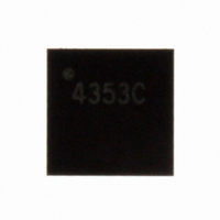
CS4353-CNZ Cirrus Logic Inc, CS4353-CNZ Datasheet - Page 7

CS4353-CNZ
Manufacturer Part Number
CS4353-CNZ
Description
IC DAC STER 106DB 2VRMS 24QFN
Manufacturer
Cirrus Logic Inc
Datasheet
1.CS4353-CNZ.pdf
(26 pages)
Specifications of CS4353-CNZ
Number Of Converters
1
Package / Case
24-QFN
Number Of Bits
24
Data Interface
Serial
Voltage Supply Source
Single Supply
Power Dissipation (max)
152mW
Operating Temperature
-40°C ~ 85°C
Mounting Type
Surface Mount
Number Of Dac Outputs
2
Resolution
24 bit
Interface Type
Serial
Supply Voltage (max)
3.47 V
Supply Voltage (min)
3.13 V
Maximum Operating Temperature
+ 125 C
Mounting Style
SMD/SMT
Maximum Power Dissipation
152 mW
Minimum Operating Temperature
- 55 C
Supply Current
10 mA
Lead Free Status / RoHS Status
Lead free / RoHS Compliant
For Use With
598-1519 - BOARD EVAL FOR CS4353 DAC
Settling Time
-
Lead Free Status / Rohs Status
Lead free / RoHS Compliant
Other names
598-1640
Available stocks
Company
Part Number
Manufacturer
Quantity
Price
Company:
Part Number:
CS4353-CNZ
Manufacturer:
CIRRUS
Quantity:
4 588
Part Number:
CS4353-CNZ
Manufacturer:
CIRRUS
Quantity:
20 000
Company:
Part Number:
CS4353-CNZR
Manufacturer:
TI
Quantity:
600
Part Number:
CS4353-CNZR
Manufacturer:
CIRRUS
Quantity:
20 000
DS803F1
DAC ANALOG CHARACTERISTICS
Test conditions (unless otherwise specified): T
CPGND = 0 V; VBIAS, VFILT+/-, and FLYP/N+/- capacitors as shown in
997 Hz sine wave at 0 dBFS; measurement bandwidth 10 Hz to 20 kHz.
Notes: 2. Measured at the output of the external LPF on AOUTx as shown in
Dynamic Performance, Fs = 48, 96, and 192 kHz (Notes 2,
Dynamic Range
Total Harmonic Distortion + Noise
Idle Channel Noise / Signal-to-Noise Ratio
Interchannel Isolation
Analog Output
Full Scale AOUTx Output Voltage
Max Current Draw from an AOUTx Pin
Interchannel Gain Mismatch
Output Offset
Gain Drift
Output Impedance
AC-Load Resistance
Load Capacitance
AOUT_REF Rejection
Analog Reference Input
AOUT_REF Input Voltage
3. One-half LSB of triangular PDF dither is added to data.
4. Measured with the specified minimum AC-Load Resistance present on the AOUTx pins.
5. Measured between the AOUTx and AOUT_REF pins.
6. External impedance between the AOUTx pin and the load will lower the voltage delivered to the load.
7. V
8. Measured with AOUT_REF connected directly to ground. External impedance between AOUT_REF
Note that for sine wave signals:
and ground will lower the AOUT_REF rejection.
PP
(Note
is the controlling specification. V
Parameter
5)
24-bit
24-bit
16-bit
16-bit A-Weighted
(Notes 4, 6, 7)
A-Weighted
(Notes 8, 9)
unweighted
unweighted
(Note 10)
(1 kHz)
-20 dB
-60 dB
-20 dB
-60 dB
(A-wt)
0 dB
0 dB
V
RMS
A
= 25 °C; VCP = VA = 3.3 V; AOUT_REF = AGND = DGND =
Symbol
I
THD+N
RMS
OUTmax
Z
AOR
=
R
C
OUT
L
L
--------- -
2 2
V
specification valid for sine wave signals only.
pp
Min
1.02
2.89
94
91
5
-
-
-
-
-
-
-
-
-
-
-
-
-
-
-
-
-
-
-
1_2VRMS = 0
3,
4)
1.08
3.05
Typ
100
100
575
100
100
115
-93
-77
-37
-93
-75
-29
0.1
97
92
89
±5
40
-
-
-
Figure 3 on page
Max
1000
1.13
3.20
-87
-71
-31
0.2
±8
-
-
-
-
-
-
-
-
-
-
-
-
-
-
-
Figure 3 on page
Min
2.04
5.78
100
97
5
-
-
-
-
-
-
-
-
-
-
-
-
-
-
-
-
-
-
-
1_2VRMS = 1
12; input test signal is a
Typ
2.15
6.09
106
103
106
115
575
100
100
-93
-83
-43
-93
-75
-35
0.1
98
95
±5
40
-
-
-
12.
Max
1000
2.26
6.40
-87
-77
-37
0.2
±8
-
-
-
-
-
-
-
-
-
-
-
-
-
-
-
CS4353
ppm/°C
V
Unit
Vpp
V
mV
dB
dB
dB
dB
dB
dB
dB
dB
dB
dB
dB
dB
μA
dB
kΩ
pF
dB
RMS
Ω
pp
7


