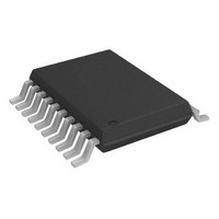
AD5428YRUZ Analog Devices Inc, AD5428YRUZ Datasheet - Page 23

AD5428YRUZ
Manufacturer Part Number
AD5428YRUZ
Description
IC DAC 8BIT DUAL MULT 20TSSOP
Manufacturer
Analog Devices Inc
Datasheet
1.AD5428YRUZ.pdf
(32 pages)
Specifications of AD5428YRUZ
Data Interface
Parallel
Settling Time
30ns
Number Of Bits
8
Number Of Converters
2
Voltage Supply Source
Single Supply
Power Dissipation (max)
3.3µW
Operating Temperature
-40°C ~ 125°C
Mounting Type
Surface Mount
Package / Case
20-TSSOP
Resolution (bits)
8bit
Sampling Rate
21.3MSPS
Input Channel Type
Parallel
Supply Voltage Range - Analogue
2.5V To 5.5V
Supply Current
500nA
Digital Ic Case Style
TSSOP
Package
20TSSOP
Resolution
8 Bit
Conversion Rate
21.3 MSPS
Architecture
R-2R
Digital Interface Type
Parallel
Number Of Outputs Per Chip
2
Output Type
Current
Full Scale Error
±25 mV
Integral Nonlinearity Error
±0.25 LSB
Maximum Settling Time
0.12 us
Lead Free Status / RoHS Status
Lead free / RoHS Compliant
For Use With
EVAL-AD5428EBZ - BOARD EVAL FOR AD5428
Lead Free Status / RoHS Status
Lead free / RoHS Compliant, Lead free / RoHS Compliant
Available stocks
Company
Part Number
Manufacturer
Quantity
Price
Part Number:
AD5428YRUZ
Manufacturer:
ADI/亚德诺
Quantity:
20 000
PCB LAYOUT AND POWER SUPPLY DECOUPLING
In any circuit where accuracy is important, careful
consideration of the power supply and ground return layout
helps to ensure the rated performance. The printed circuit
board on which the AD5428/AD5440/AD5447 is mounted
should be designed so that the analog and digital sections are
separate and confined to certain areas of the board. If the DAC
is in a system where multiple devices require an AGND-to-
DGND connection, the connection should be made at one
point only. The star ground point should be established as close
as possible to the device.
These DACs should have ample supply bypassing of 10 µF in
parallel with 0.1 µF on the supply located as close as possible to
the package, ideally right up against the device. The 0.1 µF
capacitor should have low effective series resistance (ESR) and
low effective series inductance (ESI), like the common ceramic
types of capacitors that provide a low impedance path to ground
at high frequencies, to handle transient currents due to internal
logic switching. Low ESR 1 µF to 10 µF tantalum or electrolytic
capacitors should also be applied at the supplies to minimize
transient disturbance and filter out low frequency ripple.
Components, such as clocks, that produce fast-switching signals
should be shielded with digital ground to avoid radiating noise
to other parts of the board, and they should never be run near
the reference inputs.
Avoid crossover of digital and analog signals. Traces on
opposite sides of the board should run at right angles to each
other. This reduces the effects of feedthrough on the board. A
Rev. B | Page 23 of 32
microstrip technique is by far the best method, but its use is not
always possible with a double-sided board. In this technique,
the component side of the board is dedicated to the ground
plane, and signal traces are placed on the soldered side.
It is good practice to use compact, minimum lead length PCB
layout design. Leads to the input should be as short as possible
to minimize IR drops and stray inductance.
The PCB metal traces between V
matched to minimize gain error. To maximize high frequency
performance, the I-to-V amplifier should be located as close as
possible to the device.
EVALUATION BOARD FOR THE AD5447
The evaluation board consists of an AD5447 DAC and a
current-to-voltage amplifier, the AD8065. Included on the
evaluation board is a 10 V reference, the ADR01. An external
reference may also be applied via an SMB input.
The evaluation kit consists of a CD-ROM with self-installing
PC software to control the DAC. The software simply allows the
user to write a code to the device.
POWER SUPPLIES FOR THE EVALUATION BOARD
The board requires ±12 V and +5 V supplies. The +12 V V
and −12 V V
is used to power the DAC (V
Both supplies are decoupled to their respective ground plane
with 10 μF tantalum and 0.1 μF ceramic capacitors.
SS
are used to power the output amplifier; the +5 V
AD5428/AD5440/AD5447
DD1
) and transceivers (V
REF
and R
FB
should also be
CC
).
DD


