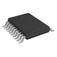
AD5428YRUZ Analog Devices Inc, AD5428YRUZ Datasheet - Page 5

AD5428YRUZ
Manufacturer Part Number
AD5428YRUZ
Description
IC DAC 8BIT DUAL MULT 20TSSOP
Manufacturer
Analog Devices Inc
Datasheet
1.AD5428YRUZ.pdf
(32 pages)
Specifications of AD5428YRUZ
Data Interface
Parallel
Settling Time
30ns
Number Of Bits
8
Number Of Converters
2
Voltage Supply Source
Single Supply
Power Dissipation (max)
3.3µW
Operating Temperature
-40°C ~ 125°C
Mounting Type
Surface Mount
Package / Case
20-TSSOP
Resolution (bits)
8bit
Sampling Rate
21.3MSPS
Input Channel Type
Parallel
Supply Voltage Range - Analogue
2.5V To 5.5V
Supply Current
500nA
Digital Ic Case Style
TSSOP
Package
20TSSOP
Resolution
8 Bit
Conversion Rate
21.3 MSPS
Architecture
R-2R
Digital Interface Type
Parallel
Number Of Outputs Per Chip
2
Output Type
Current
Full Scale Error
±25 mV
Integral Nonlinearity Error
±0.25 LSB
Maximum Settling Time
0.12 us
Lead Free Status / RoHS Status
Lead free / RoHS Compliant
For Use With
EVAL-AD5428EBZ - BOARD EVAL FOR AD5428
Lead Free Status / RoHS Status
Lead free / RoHS Compliant, Lead free / RoHS Compliant
Available stocks
Company
Part Number
Manufacturer
Quantity
Price
Part Number:
AD5428YRUZ
Manufacturer:
ADI/亚德诺
Quantity:
20 000
TIMING CHARACTERISTICS
All input signals are specified with tr = tf = 1 ns (10% to 90% of V
V
Table 2.
Parameter
Write Mode
Data Readback Mode
Update Rate
1
Guaranteed by design and characterization, not subject to production test.
REF
t
t
t
t
t
t
t
t
t
t
t
t
t
1
2
3
4
5
6
7
8
9
10
11
12
13
= 10 V, I
1
OUT
2 = 0 V, temperature range for Y version: −40°C to +125°C. All specifications T
DACA/DACB
DATA
R/W
Limit at T
0
0
10
10
0
6
0
5
7
0
0
5
25
5
10
21.3
CS
MIN
, T
TO OUTPUT
t
1
MAX
Figure 3. Load Circuit for Data Output Timing Specifications
PIN
DATA VALID
t
3
t
8
t
Unit
ns min
ns min
ns min
ns min
ns min
ns min
ns min
ns min
ns min
ns typ
ns typ
ns typ
ns max
ns typ
ns max
MSPS
4
C
50pF
L
Figure 2. Timing Diagram
200µA
200µA
Rev. B | Page 5 of 32
t
t
2
5
DD
t
7
) and timed from a voltage level of (V
I
I
OH
OL
t
9
t
8
t
V
10
OH (MIN)
Conditions/Comments
R/W to CS setup time
R/W to CS hold time
CS low time
Address setup time
Address hold time
Data setup time
Data hold time
R/W high to CS low
CS min high time
Address setup time
Address hold time
Data access time
Bus relinquish time
Consists of CS min high time, CS low time, and output
voltage settling time
+ V
t
2
12
OL (MAX)
DATA VALID
t
11
MIN
to T
AD5428/AD5440/AD5447
MAX
t
IL
13
t
, unless otherwise noted.
2
+ V
IH
)/2. V
DD
= 2.5 V to 5.5 V,


