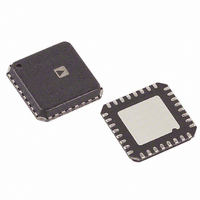
AD9704BCPZ Analog Devices Inc, AD9704BCPZ Datasheet - Page 39

AD9704BCPZ
Manufacturer Part Number
AD9704BCPZ
Description
IC DAC TX 8BIT 175MSPS 32-LFCSP
Manufacturer
Analog Devices Inc
Series
TxDAC®r
Datasheet
1.AD9704BCPZ.pdf
(52 pages)
Specifications of AD9704BCPZ
Data Interface
Serial
Settling Time
11ns
Number Of Bits
8
Number Of Converters
1
Voltage Supply Source
Analog and Digital
Power Dissipation (max)
50mW
Operating Temperature
-40°C ~ 85°C
Mounting Type
Surface Mount
Package / Case
32-LFCSP
Resolution (bits)
8bit
Sampling Rate
175MSPS
Input Channel Type
Parallel
Supply Current
5.1mA
Digital Ic Case Style
CSP
No. Of Pins
32
Supply Voltage Range - Analogue
3.3V To 3.6V
Rohs Compliant
Yes
Number Of Channels
1
Resolution
8b
Interface Type
Parallel
Single Supply Voltage (typ)
1.8/3.3V
Architecture
Segment
Power Supply Requirement
Analog and Digital
Output Type
Current
Integral Nonlinearity Error
±0.09LSB
Single Supply Voltage (min)
1.7V
Single Supply Voltage (max)
3.6V
Operating Temp Range
-40C to 85C
Operating Temperature Classification
Industrial
Mounting
Surface Mount
Pin Count
32
Package Type
LFCSP EP
Lead Free Status / RoHS Status
Lead free / RoHS Compliant
Lead Free Status / RoHS Status
Lead free / RoHS Compliant, Lead free / RoHS Compliant
Available stocks
Company
Part Number
Manufacturer
Quantity
Price
Company:
Part Number:
AD9704BCPZ
Manufacturer:
Analog Devices Inc
Quantity:
135
Company:
Part Number:
AD9704BCPZ
Manufacturer:
FREESCAL
Quantity:
2
Part Number:
AD9704BCPZ
Manufacturer:
ADI/亚德诺
Quantity:
20 000
The calibration clock frequency is equal to the DAC clock
divided by the division factor chosen by the DIVSEL value. The
frequency of the calibration clock must be set to under 10 MHz
for reliable calibrations. Best results are obtained by setting
DIVSEL[2:0] (Register 0x0E, Bit 2 to Bit 0) to produce the
lowest frequency calibration clock frequency that the user’s
system requirements allow.
To perform a device self-calibration, the following procedure
can be used.
1.
2.
3.
4.
5.
6.
The AD9704/AD9705/AD9706/AD9707 devices allow reading and
writing of the calibration coefficients. There are 33 coefficients in
total. The read/write feature of the coefficients can be useful for
improving the results of the self-calibration routine by averaging
the results of several calibration results and loading the aver-
aged results back into the device. The reading and writing
routines follow.
Enable the calibration clock by setting the CALCLK bit
(Register 0x02, Bit 0).
Enable self-calibration by writing 0x40 to Register 0x0F.
Wait approximately 4500 calibration clock cycles. Each
calibration clock cycle is between 2 and 256 DAC clock
cycles, depending on the value of DIVSEL[2:0].
Check if the self-calibration has completed by reading the
CALSTAT bit (Register 0x0F, Bit 7). A Logic 1 indicates the
calibration has completed.
When the self-calibration has completed, write 0x00 to
Register 0x0F.
Disable the calibration clock by clearing the CALCLK Bit
(Register 0x02, Bit 0).
Rev. A | Page 39 of 52
To read the calibration coefficients:
1.
2.
3.
4.
5.
6.
7.
To write the calibration coefficients to the device:
1.
2.
3.
4.
5.
6.
7.
Enable the calibration clock by setting the CALCLK bit
(Register 0x02, Bit 0).
Write the address of the first coefficient (0x00) to
Set the SMEMRD bit (Register 0x0F, Bit 2) by writing 0x04
Read the value of the first coefficient by reading the
Clear the SMEMRD bit by writing 0x00 to Register 0x0F.
Repeat Step 2 through Step 5 for each of the remaining
Disable the calibration clock by clearing the CALCLK Bit
(Register 0x02, Bit 0).
Enable the calibration clock by setting the CALCLK bit
(Register 0x02, Bit 0).
Set the SMEMWR bit (Register 0x0F, Bit 3) by writing 0x08
Write the address of the first coefficient (0x00) to
Write the value of the first coefficient to Register 0x11.
Repeat Step 2 and Step 3 for each of the remaining
Clear the SMEMWR bit by writing 0x00 to Register 0x0F.
Disable the calibration clock by clearing the CALCLK bit
Register 0x10.
to Register 0x0F.
contents of Register 0x11.
32 coefficients by incrementing the address by one for
each read.
to Register 0x0F.
Register 0x10.
32 coefficients by incrementing the address by one for
each write.
(Register 0x02, Bit 0).
AD9704/AD9705/AD9706/AD9707


