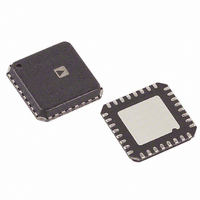
AD9704BCPZ Analog Devices Inc, AD9704BCPZ Datasheet - Page 9

AD9704BCPZ
Manufacturer Part Number
AD9704BCPZ
Description
IC DAC TX 8BIT 175MSPS 32-LFCSP
Manufacturer
Analog Devices Inc
Series
TxDAC®r
Datasheet
1.AD9704BCPZ.pdf
(52 pages)
Specifications of AD9704BCPZ
Data Interface
Serial
Settling Time
11ns
Number Of Bits
8
Number Of Converters
1
Voltage Supply Source
Analog and Digital
Power Dissipation (max)
50mW
Operating Temperature
-40°C ~ 85°C
Mounting Type
Surface Mount
Package / Case
32-LFCSP
Resolution (bits)
8bit
Sampling Rate
175MSPS
Input Channel Type
Parallel
Supply Current
5.1mA
Digital Ic Case Style
CSP
No. Of Pins
32
Supply Voltage Range - Analogue
3.3V To 3.6V
Rohs Compliant
Yes
Number Of Channels
1
Resolution
8b
Interface Type
Parallel
Single Supply Voltage (typ)
1.8/3.3V
Architecture
Segment
Power Supply Requirement
Analog and Digital
Output Type
Current
Integral Nonlinearity Error
±0.09LSB
Single Supply Voltage (min)
1.7V
Single Supply Voltage (max)
3.6V
Operating Temp Range
-40C to 85C
Operating Temperature Classification
Industrial
Mounting
Surface Mount
Pin Count
32
Package Type
LFCSP EP
Lead Free Status / RoHS Status
Lead free / RoHS Compliant
Lead Free Status / RoHS Status
Lead free / RoHS Compliant, Lead free / RoHS Compliant
Available stocks
Company
Part Number
Manufacturer
Quantity
Price
Company:
Part Number:
AD9704BCPZ
Manufacturer:
Analog Devices Inc
Quantity:
135
Company:
Part Number:
AD9704BCPZ
Manufacturer:
FREESCAL
Quantity:
2
Part Number:
AD9704BCPZ
Manufacturer:
ADI/亚德诺
Quantity:
20 000
DIGITAL SPECIFICATIONS (1.8 V)
T
Table 6.
Parameter
DIGITAL INPUTS
CLK INPUTS
1
2
TIMING DIAGRAM
Includes CLK+ pin in single-ended clock input mode.
Applicable to CLK+ input and CLK– input when configured for differential clock input mode.
MIN
Logic 1 Voltage
Logic 0 Voltage
Logic 1 Current
Logic 0 Current
Input Capacitance
Input Setup Time (t
Input Hold Time (t
Input Setup Time (t
Input Hold Time (t
Latch Pulse Width (t
Input Voltage Range
Common-Mode Voltage
Differential Voltage
to T
−40°C to +85°C
−40°C to +85°C
MAX
2
, AVDD = 1.8 V, DVDD = 1.8 V, CLKVDD = 1.8 V, I
1
H
H
); 25°C
);
S
S
); 25°C
);
LPW
)
Min
2.3
0
6.2
1.2
−
2.4
0.1
0
0.4
0.5
DBO TO DB13
10
CLOCK
IOUTA
IOUTB
AD9707
Typ
1.8
0
5
0.9
1.5
OR
Max
0.5
+10
+10
1.8
1.3
t
S
Min
1.2
−
2.3
0
2.4
0.1
6.2
0
0.4
0.5
Figure 2. Timing Diagram
10
Rev. A | Page 9 of 52
t
PD
OUTFS
AD9706
Typ
1.8
0
5
0.9
1.5
= 1 mA, unless otherwise noted.
0.1%
t
t
ST
LPW
Max
0.5
+10
+10
1.8
1.3
t
H
Min
1.2
−
2.3
0
2.4
0.1
6.2
0
0.4
0.5
0.1%
10
AD9704/AD9705/AD9706/AD9707
AD9705
Typ
1.8
0
5
0.9
1.5
Max
0.5
+10
+10
1.8
1.3
Min
1.2
−
2.3
0
2.4
0.1
6.2
0
0.4
0.5
10
AD9704
Typ
1.8
0
5
0.9
1.5
Max
0.5
+10
+10
1.8
1.3
Unit
V
V
μA
μA
pF
ns
ns
ns
ns
ns
V
V
V


